
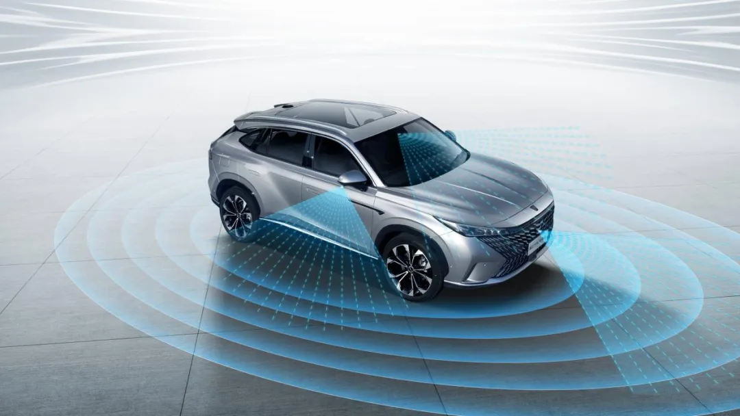
To enhance user experience with advanced intelligent driving features, SAIC Roewe has invested significant effort in the overall vehicle perception sensor scheme. The new third-generation Roewe RX5 NGP intelligent driving version adopts a multi-dimensional perception fusion scheme, equipped with one 8-megapixel 120° front-view camera, five 2-megapixel 100° surround-view cameras, four 360° panoramic cameras, three millimeter-wave radars, twelve ultrasonic radars, and a high-precision positioning module, totaling 28 sensors, providing comprehensive coverage of the vehicle’s surroundings, achieving a longer detection distance, wider detection range, and more accurate identification of various objects.
To realize multi-sensor fusion and more complex algorithms, the Roewe NGP intelligent driving version domain controller is provided by Horizon Robotics, utilizing three Horizon Journey 3 high-performance domestic AI chips, which employ Horizon’s self-developed Bernoulli 2.0 BPU® architecture to implement various intelligent driving algorithm modules such as environmental perception, map positioning, and fusion planning, achieving 360° surround vision perception coverage. Furthermore, this system supports efficient intelligent driving planning and decision-making algorithms, possesses deep learning capabilities, and offers iterative update functions.
1. Appearance Structure of Intelligent Driving Domain Controller
The Roewe RX5 NGP intelligent driving version domain controller is designed by Horizon Robotics. The shell is made of metal machining, with numerous heat dissipation grooves on the surface. This domain controller adopts a natural heat dissipation method for thermal management, with thermal grease applied to the main chip surface, making direct contact with the metal columns extending inside the metal shell, thereby dissipating heat through the shell connected to the metal columns to the outside. The heat dissipation grooves on the outer shell can increase the contact area with air, facilitating better heat dissipation for the domain controller.
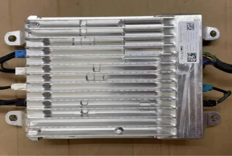
Front View of the Intelligent Driving Domain Controller Shell
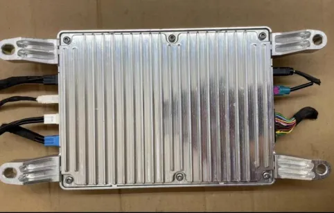
Back View of the Intelligent Driving Domain Controller Shell
2. Interfaces of the Intelligent Driving Domain Controller
The wiring terminals of this domain controller are distributed on both sides; the right side mainly contains power, IO, communication interfaces, GPS antenna, etc.; the left side mainly houses the harness terminals for surround view, panoramic view, and front view.
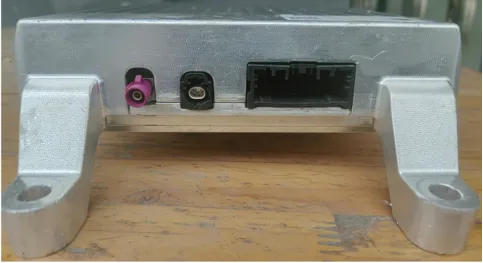
Wiring Terminal Diagram 1 of the Intelligent Driving Domain Controller
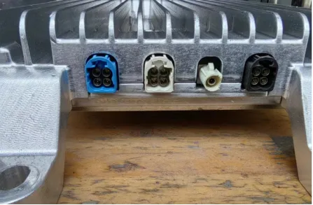
Wiring Terminal Diagram 2 of the Intelligent Driving Domain Controller
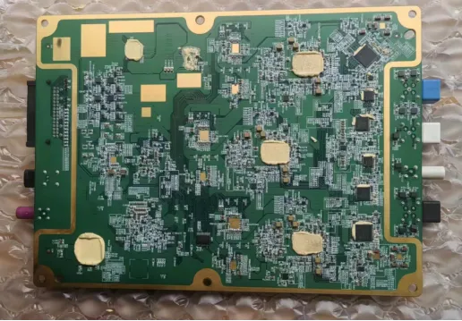
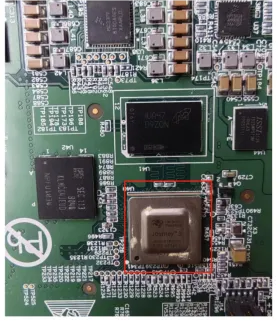
3. PCB of the Intelligent Driving Domain Controller
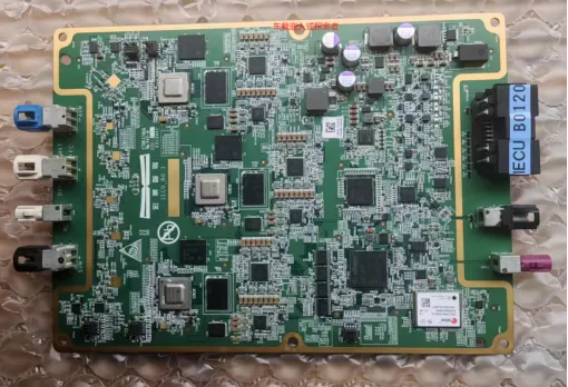
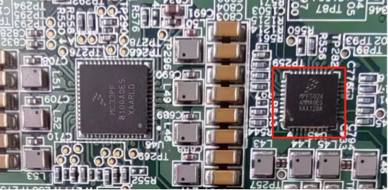
Front View of the Autonomous Driving Domain Controller PCB
Annotated Front View of the Autonomous Driving Domain Controller PCB
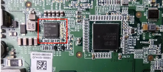
The numbers in the figure are as follows: 1-Horizon J3, 2-Micron DDR4 2G, 3-Samsung eMMC 64G, 4-American Chip NOR flash, 5-Infineon AURIX TC397, 6-Ublox ZED F9K, 7-NXP Switch SJA1105Q, 8-Power Chip MC33PF 8100A0ES, 9-Power Chip Infineon 355584, 10-PHY Chip RTL9010AA, 12-Power Management Chip MPF5024AMMA0ES.
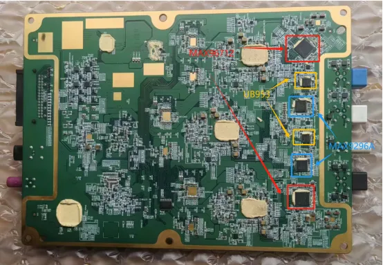
Annotated Back View of the Autonomous Driving Domain Controller PCB
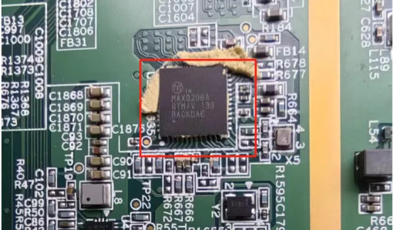
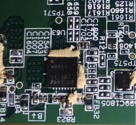
The numbers in the figure are as follows: Maxim GMSL MAX96712, Texas Instruments FDLink UB953, Maxim GMSL MAX9296A.
4. Domain Controller System
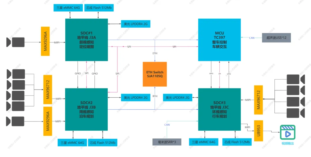
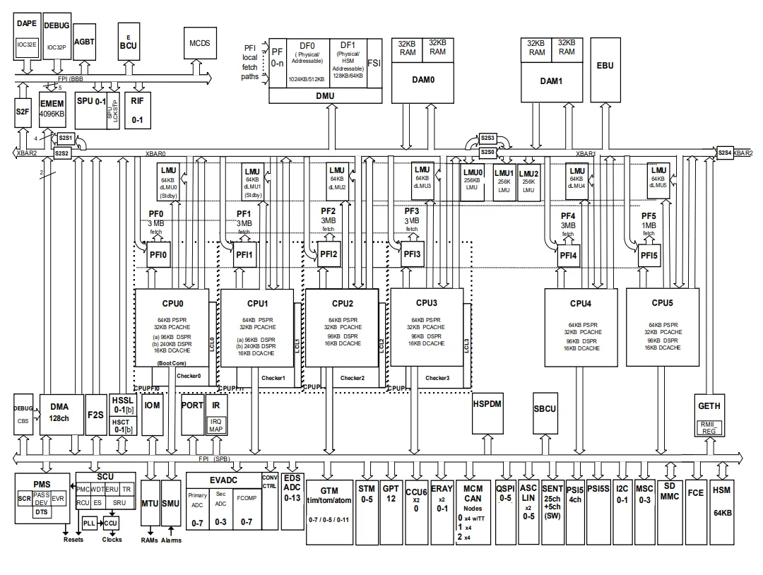
System Block Diagram of the Autonomous Driving Domain Controller
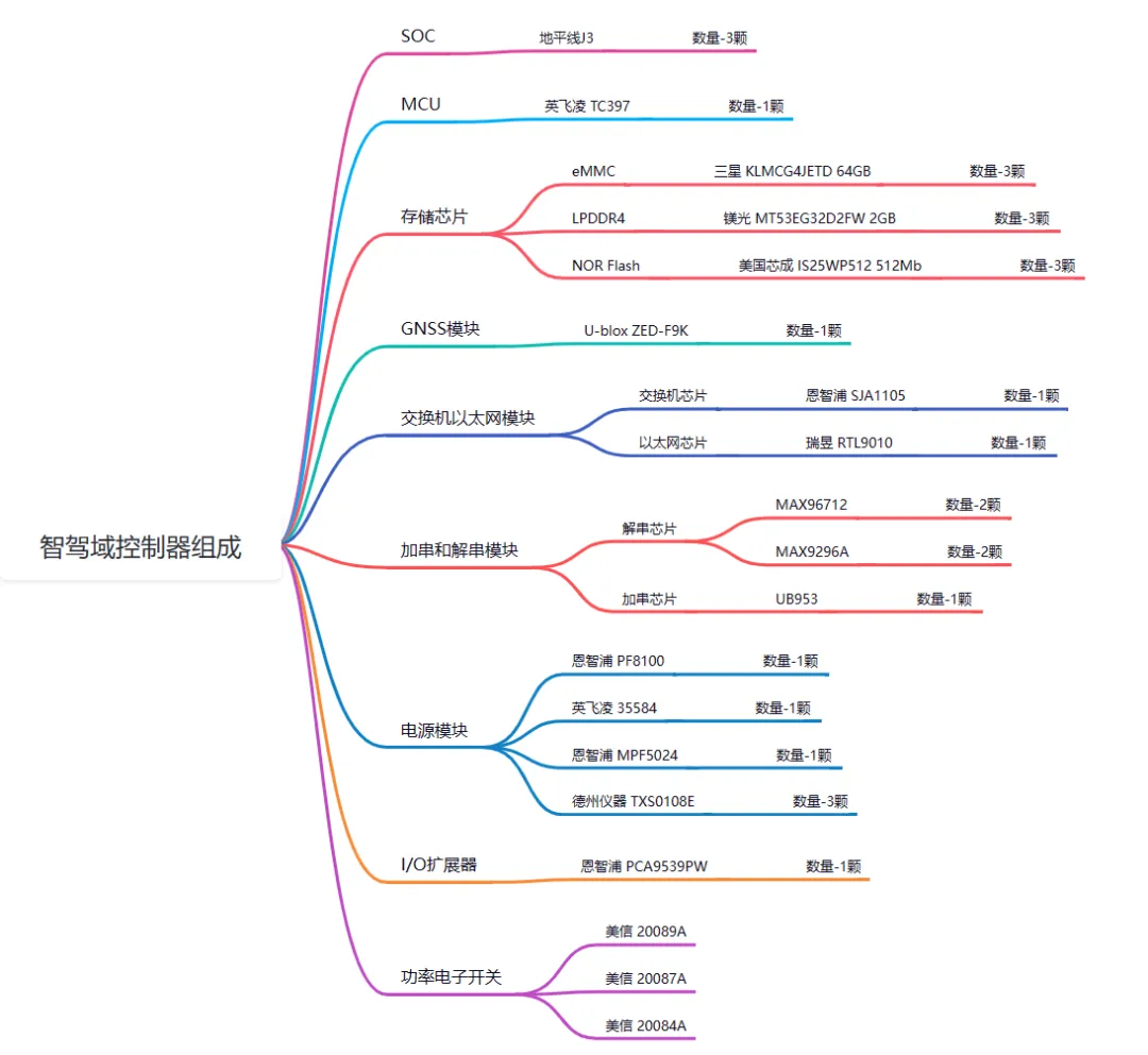
Composition Diagram of the Autonomous Driving Domain Controller
5. SOC Chips
SOC, or System on Chip, is a large integrated circuit that integrates multiple functional modules such as processor cores, memory controllers, and peripheral controllers. In the autonomous driving domain controller, the SOC chip is responsible for processing sensor data, performing real-time image processing, and executing computer vision algorithms. Common SOC chip models include NVIDIA Drive Orin, Intel’s Mobileye EyeQ series, Qualcomm’s Snapdragon Automotive Platform series, and Horizon Journey series.
This time, the Roewe RX5 uses three Horizon J3 chips.
5.1. Functions of Three Horizon J3 Chips
|
Chip Number |
Function |
|
J3-A |
Responsible for perception from the front-view camera and GNSS module for mapping and localization. |
|
J3-B |
Responsible for perception from the surround-view camera, rear-view camera, and parking planning functions. |
|
J3-C |
Responsible for perception from the four surround-view cameras and driving planning functions. |
5.2. Introduction to Horizon Journey 3 Chip
The Horizon Journey 3 is the second-generation vehicle-mounted intelligent chip from Horizon; it is based on Horizon’s self-developed BPU®️2.0 architecture and meets AEC-Q100 standards. The Journey 3 not only supports deep learning-based image detection, classification, and pixel-level segmentation functions but also supports efficient encoding of H.264 and H.265 video formats, making it an ideal platform for performing complex multi-channel computing tasks and multi-channel digital video recording, such as enabling advanced driver-assistance systems (ADAS) and automated parking assistance (APA).
5.3. Features of Horizon Journey 3
|
General Characteristics |
· Manufactured using TSMC’s 16nm FFC process; · Utilizes FCBGA484 packaging with a pin pitch of 0.65mm, chip size of 15mmx15mm; · Complies with automotive AEC-Q100 Grade 2 standards (operating temperature: -40~105 degrees Celsius) |
|
CPU Characteristics |
· Features four Arm Cortex A53 cores with 32KB/32KB L1 I/D cache and 512KB of L2 cache; · Maximum operating frequency: 1.2GHz; · Supports Dynamic Frequency Scaling (DFS); |
|
BPU Characteristics |
· Composed of BPU0 core and BPU1 dual-core Bernoulli architecture, with a computing power of 5TOPS; · Maximum operating frequency: 950MHz; · Supports Dynamic Frequency Scaling (DFS); |
|
DDR Characteristics |
· Supports x32 external DDR4/LPDDR4/LPDDR4X DRAM, with a maximum capacity of 4GB; · The maximum speed supported by DDR4 can reach DDR4-3200 MT/s; · The maximum speed supported by LPDDR4/LPDDR4X can reach 3200MT/s; |
|
Network Interface Characteristics |
· Supports one Gigabit Ethernet interface; · External Ethernet PHY supports RMII and RGMII protocols; · Supports Time-Sensitive Networking (TSN) and Audio Video (AV) traffic; |
|
Host Interface |
· Uses BIF-SPI slave interface, with a maximum transfer rate of 66 MHz for AP SPI master device; · Suitable for AP eMMC main device transfer mode, with a maximum of 8 lines using BIF-SD device interface in HS200 mode (maximum 192MB/s). The application processor (AP) accesses J3’s DDR, SRAM, and module registers for data exchange and control via BIF-SPI and BIF-SD main interfaces; · Supports USB3.0 host/device dual-role high-speed interface. |
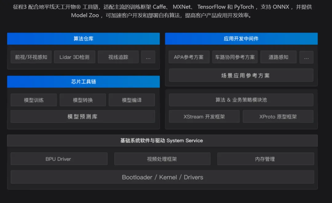
5.4. Toolchain for Horizon Journey 3
6. Storage Chips
Common storage modules used in intelligent driving domain controllers include eMMC and DDR4; they play an important role in storing data within the autonomous driving domain controller. The eMMC chip, as a flash storage device, is responsible for storing the operating system, algorithms, and data of the system. The DDR4 chip, on the other hand, is a high-speed memory chip responsible for caching and running algorithms. Common eMMC chip models include Samsung’s KLM and SK Hynix’s eMMC, while common DDR4 chip models include Micron’s Crucial and Kingston’s HyperX.
6.1. DDR4
Micron DDR4 2GB, specific model: MT53E1G32D2FW-046
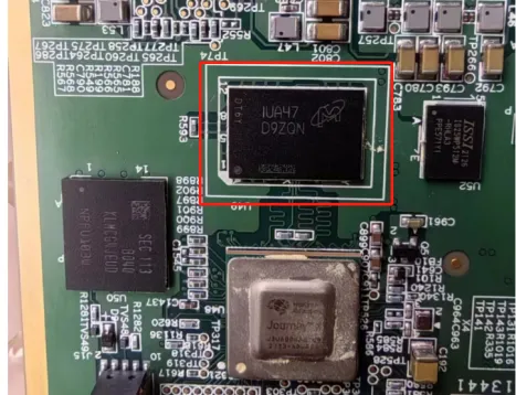
6.2. eMMC
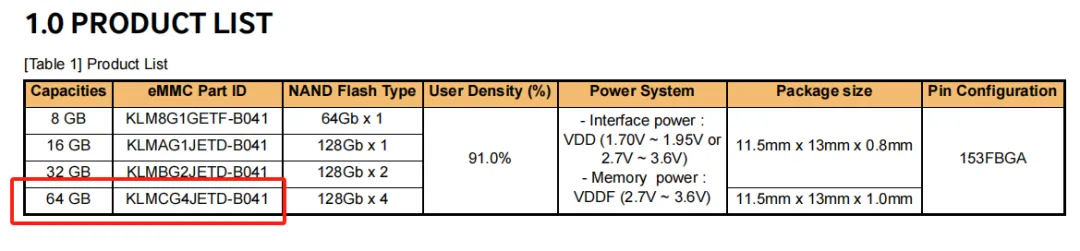
Model: KLMCG4JETD-B041, Samsung eMMC 64G
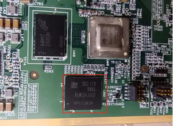
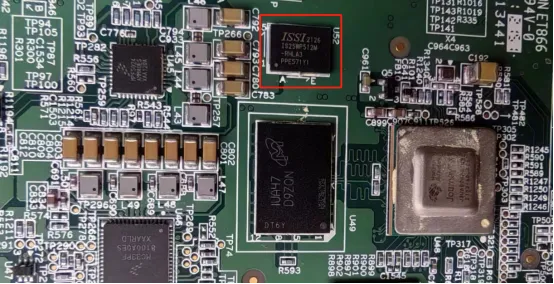
6.3. NOR FLASH
American Chip IS25WP512M-RHLA3 512Mb
7. MCU Chips
The MCU chip plays an important role in the autonomous driving domain controller. MCU, or Microcontroller Unit, is a microcomputer that integrates processor cores, memory, input/output interfaces, and other functions. In the autonomous driving domain controller, the MCU chip is responsible for real-time computing, data acquisition, and control tasks. Common MCU chip models include NXP’s S32K series, Infineon’s AURIX TC3X7 series, and Renesas’s RH850 series. The MCU chip can communicate with the SOC chip via CAN bus, Ethernet, and SPI.
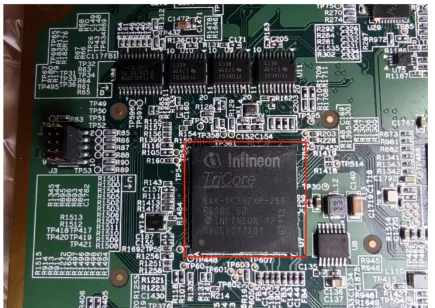
The TC397 chip in this domain controller is responsible for overall vehicle control and data interaction.
Introduction to Infineon’s AURIX TC397
The TC397 belongs to Infineon’s AURIX 2G series products, which feature a high-performance architecture with up to six cores, achieving a maximum clock frequency of 300MHz and enabling high-speed computing capabilities. In terms of storage, this series supports up to 16MB Flash and features A/B switching functionality, facilitating convenient over-the-air software updates (SOTA); in terms of functional safety, this series can be equipped with up to four lockstep cores, complying with ISO 26262 functional safety level D; it also integrates a hardware security module (HSM), making it very suitable for the autonomous driving field.
TC397 Features
|
Features |
Cores: 6 TriCore™ running at 300 MHz (with 4 lockstep cores providing 4000 DMIPS) Flash: 16 MB Flash/ECC protection RAM: Up to 6.9 MB SRAM/ECC protection PHY: 1 Gbit Ethernet Peripherals: 12xCAN FD, 2xFlexRay, 12xLINs, 4xQSP, 2xI²C, 25xSENT, 6xPSI, 2xHSSL, 4xMSC, 1x eMMC/SDIO LVDS: 8×400 Mbit/s LVDS radar interface SPU: 2x SPU (Signal Processing Units) for radar signal processing Timers: Redundant and diverse timer modules (GTM, CCU6, GPT12) Encryption: Complete HSM (ECC256 and SHA2) Packaging: BGA-292 package Functional Safety: Developed and documented according to ISO 26262/IEC61508 to support safety requirements up to ASIL-D/SIL3 AUTOSAR: AUTOSAR 4.2 support Power Supply: Single voltage supply of 5 V or 3.3 V Temperature: 165°C junction temperature |
8. Serializer/Deserializer Chips
8.1. MAX96712
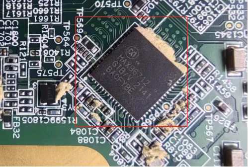
Introduction to MAX96712
MAX96712 deserializer converts GMSL2 or GMSL1 serial input into MIPI CSI-2 D-PHY or C-PHY format output. This device allows simultaneous transmission of bidirectional control channel data while video transmission is ongoing for each link. The MAX96712 can accommodate up to four remote sensors using standard coaxial cables or STP interconnects. Each GMSL2 serial link operates at a fixed rate of 3Gbps or 6Gbps in the forward direction and at 187.5Mbps in the reverse direction. In GMSL1 mode, the MAX96712 can be paired with first-generation GMSL1 serializers operating at 3.12Gbps or 1.5Gbps, or operate with GMSL2 serializers at up to 3.12Gbps.
MAX96712 supports aggregation and duplication of video data, allowing data streams from multiple remote sensors to be combined and routed to one or more available CSI-2 outputs. Data can also be routed so that multiple streams from a single GMSL input can be routed independently to different CSI-2 outputs. Alternatively, frame-level cascading can be used to synchronize and combine data from multiple sensors into a single CSI-2 stream within a composite superframe. The CSI-2 interface supports 2x 4-channel and 4x 2-channel configurations using C-PHY or D-PHY.
Various peripheral communication options are provided for flexible local register access and remote device programming. Three I2C/UART ports support redundant local and remote internal register access for parallel or tunneled remote peripheral communication. Additionally, two SPI ports are provided as tunneled interfaces to remote peripherals (GMSL2).
Features of MAX96712
|
Features |
Details |
|
MIPI CSI-2 v1.3 output configurable as 2×4 channels, 1×4 lane + 2×2 lanes, or 4×2 lanes
|
• Optional D-PHY v1.2, 80Mbps to 2.5Gbps/channel or C-PHY v1.0, 182Mbps to 5.7Gbps/channel • 16/32 channel virtual channel support (D/C-PHY) • Flexible aggregation and routing of incoming data through CSI-2 VC or frame-level cascading • Data can be duplicated and routed to any CSI port • Supports RAW8/10/12/14/16/20, RGB565/666/888, YUV422 8/10 bit formats • Dual-pixel mode to improve transmission efficiency • CSI-2 lane reassignment and polarity inversion • MIPI/GMSL video PRBS generator and checker • Checkerboard/color gradient pattern generator • Raw CSI-2 PRBS generator • Independently configure all video paths and GMSL/CSI-2 ports |
|
Four independent GMSL inputs with independently configurable GMSL1/2 operation, link speeds, and video formats
|
• Mixed support for GMSL1/GMSL2 and 3G/6G • Backward compatible with GMSL1 serializers • GMSL1 forward link speeds up to 3.12Gbps • GMSL2 link speeds of 3Gbps or 6Gbps (forward) and 187.5Mbps (reverse) • Synchronization and simultaneous support for asynchronous cameras • Achieves precise synchronization of multiple serializers in large camera systems • GMSL PRBS generator/checker for link testing • Eye monitor for continuous diagnostics • Adaptive equalization for up to 15 meters of coaxial cable with multiple inline connectors • Compatible with 50Ω coaxial cables or 100Ω STP |
|
ASIL-B compliant (GMSL2)
|
• Video watermark insertion and detection • 16-bit CRC protection for control channel data with retransmission upon error detection • Optional 32-bit CRC protection for video line data • ECC protection for video data memory • CRC protection for CSI-2 data streams |
|
Concurrent control channels for device configuration and communication with remote peripherals |
• 3 I2C/UART, 2 SPI, 17 GPIO • Eight hardware selectable device addresses |
|
Programmable spread spectrum reduces EMI |
|
|
64-pin 9mm x 9mm TQFN with exposed pads |
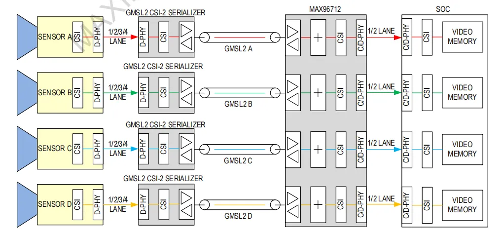
System Diagram of MAX96712 with Four Independent Inputs and Outputs
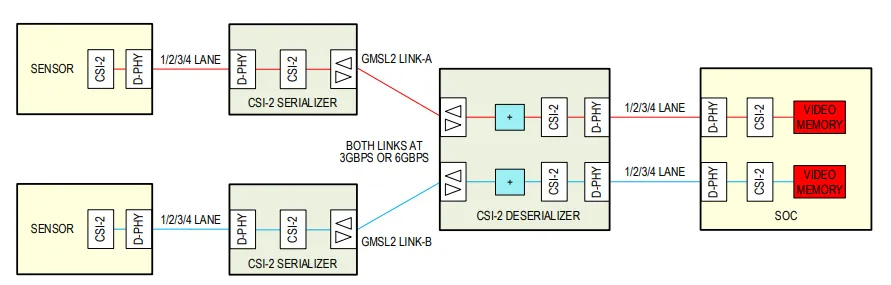
8.2. MAX9296A
MAX9296A deserializer converts single or dual serial inputs into MIPI CSI-2 output. This device operates in GMSL1 or GMSL2 mode. MAX9296A also sends and receives side channel data, enabling full-duplex transmission of forward path video and bidirectional control data, using 50Ω coaxial cable or 100Ω STP cable compliant with GMSL2 or GMSL1 channel specifications.
Physical Diagram of MAX9296A
Block Diagram of Two Independently Operating Video Sources of MAX9296A
8.3. UB953
Introduction to UB953
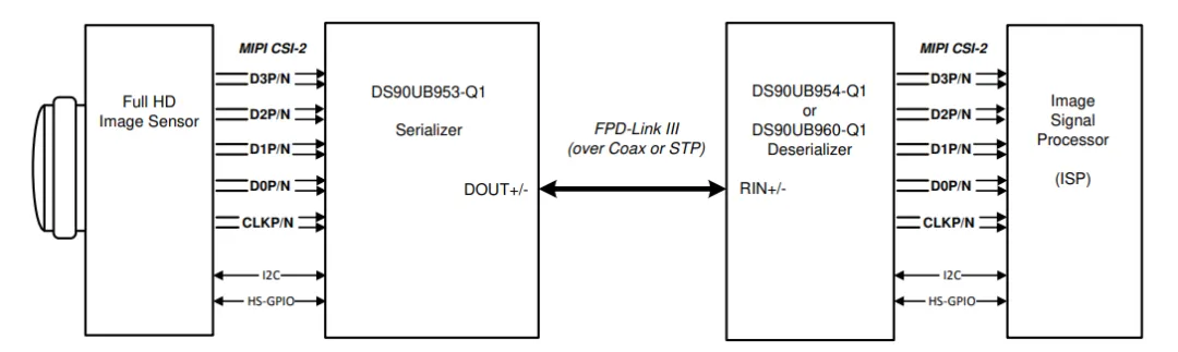
DS90UB953-Q1 serializer belongs to the TI FPD-Link III device series, designed to support high-speed raw data sensors, including 2.3MP/60fps imagers and 4MP/30fps cameras, satellite radars, lidar, and time-of-flight (ToF) sensors. This chip provides a 4.16Gbps forward channel and ultra-low latency 50Mbps bidirectional control channel, and supports power over coax (PoC) or STP cable. When combined with the accompanying deserializer, DS90UB953-Q1 can provide precise multi-camera sensor clock and sensor synchronization.
Features of UB953
|
Features |
• Complies with automotive AEC-Q100 standards: – Device temperature grade 2: environmental operating temperature range of -40°C to +105°C; • Complies with ISO 10605 and IEC 61000-4-2 ESD standards; • Coaxial cable power (PoC) compatible transceiver; • 4.16Gbps level serializer supports high-speed sensors, including full HD 1080p 2.3MP 60fps and 4MP 30fps imagers; • System interface compliant with D-PHY v1.2 and CSI-2 v1.3 standards – up to 4 data channels, each with a rate of 832Mbps – supports up to four virtual channels • Precision multi-camera clock and synchronization • Flexible programmable output clock generator • Advanced data protection and diagnostics, including CRC data protection, sensor data integrity checks, I2C write protection, voltage and temperature measurements, programmable alarms, and line fault detection • Supports single-ended coax or shielded twisted pair (STP) cable • Ultra-low latency bidirectional I2C and GPIO control channels support ISP control from the ECU side • 1.8V single power supply • Low power consumption (0.28W typical) • Provides functional safety – documentation to assist in ISO 26262 system design • Compatible with DS90UB954-Q1, DS90UB964-Q1, DS90UB962-Q1, DS90UB936-Q1, DS90UB960-Q1, DS90UB934-Q1, and DS90UB914A-Q1 deserializers • Wide temperature range: -40°C to 105°C • Compact 5mm × 5mm VQFN package and PoC solution size, suitable for compact camera module designs |
|
Applications |
• Advanced Driver Assistance Systems (ADAS) – Surround View Systems (SVS) – Camera Monitoring Systems (CMS) – Front View Cameras (FC) – Driver Monitoring Systems (DMS) – Rear View Cameras (RVC) – Automotive Satellite Radar and Lidar Modules – Time-of-Flight (ToF) Sensors • Security and Surveillance Cameras • Industrial and Medical Imaging |
Typical Applications of UB953
9. Ethernet/Switch Chips
9.1. SJA1105Q
Introduction
SJA1105P/Q/R/S is designed to provide a cost-optimized and flexible solution for automotive Ethernet switches. The SJA1105P/Q variants are functionally enhanced versions of SJA1105/T, serving as plug-and-play alternatives. In the SJA1105R/S variants, one port provides SGMII functionality. These devices can be used in applications requiring SGMII connectivity to the host processor or applications needing to cascade multiple devices.
The SJA1105P/Q/R/S series of automotive Gigabit Ethernet switches enhances the functionality of the SJA1105/SJA1105T switches with improved safety-related features, extended interface options, and ISO 26262 ASIL-A compliance.
SJA1105P/Q/R/S is a 5-port automotive Ethernet switch that supports IEEE Audio Video Bridging (AVB) and Time-Sensitive Networking (TSN) standards. Each of the five ports can be independently configured to operate at 10/100/1000 Mbit/s. This feature provides flexibility to connect any fast/Gigabit/optical PHY or MCU/MPU to any port. Examples of external PHYs include NXP Semiconductors’ TJA1100 and TJA1102 IEEE 100BASE-T1 PHY.
All SJA1105P/Q/R/S variants offer new frame whitelist/blacklist, port reachability, and address learning limitation features, which enhance the security of the switch by restricting data processing to known frames and data sources, preventing erroneous or malicious data from being forwarded.
The updated MII/RMII/RGMII interfaces provide extended IO voltages such as 1V8 and 3V3 RGMII. Additionally, the SGMII interface available on the /R and /S variants expands the switch’s connectivity options. The /P and /Q variants do not have SGMII ports and maintain 100% pin compatibility with SJA1105/SJA1105T switches.
The SJA1105P/Q/R/S switch series is developed according to ISO 26262 standards. ASIL-A compliance reduces the design burden for safety-critical ECUs. Additional documentation, including safety manuals, can be provided upon request.
These switches are compatible with IEEE AVB standards. The /Q and /S variants support extended TSN features such as 802.1Qbv. NXP’s native AUTOSAR drivers and AVB SW stack are available for this series.
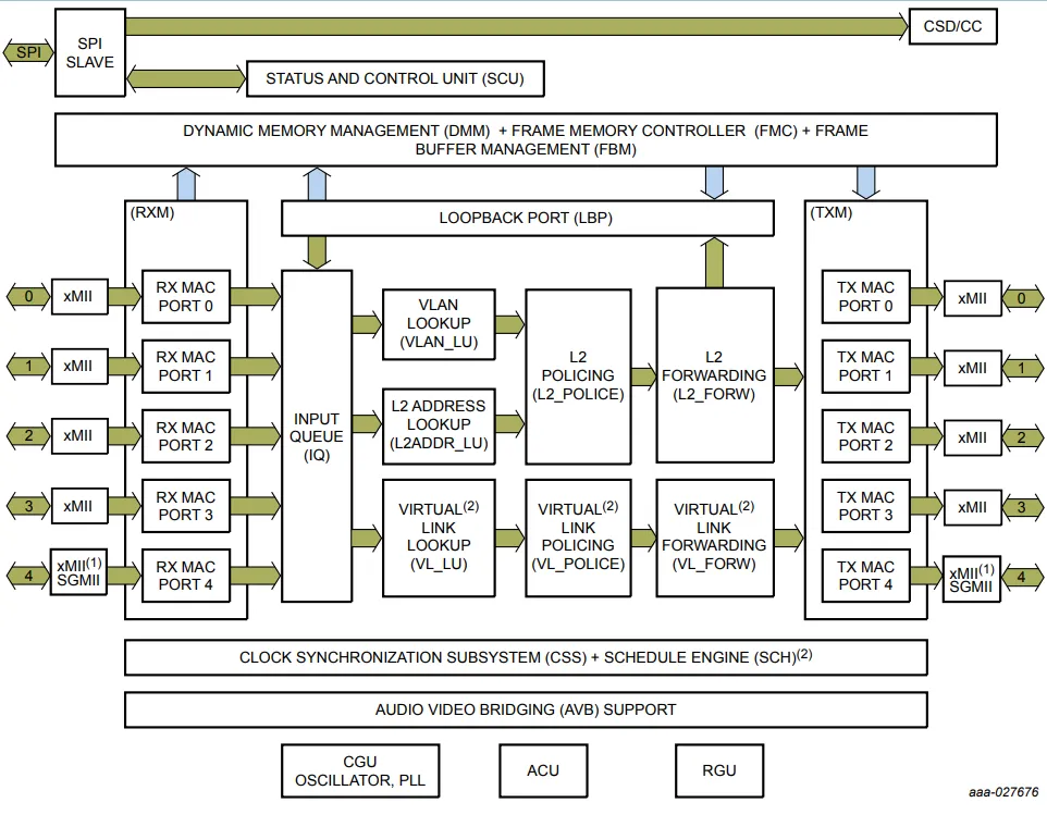
System Diagram of SJA1105 Switch Connected to PHY and Host Processor
9.2. Ethernet Chips
RTL9010AA
Introduction
RT9010 is a low-noise, low-loss product with a power capability of up to 300mA and a power-on reset function. It operates with an input range from 2.5V to 5.5V, with an output voltage range from 1.2V to 3.6V.
RT9010 features 2% accuracy, extremely low dropout (240mV@300mA), and very low ground current. The shutdown current is close to zero, making it suitable for battery-powered devices. Other features include current limiting, over-temperature, and output short-circuit protection.
RT9010 includes a short-circuit thermal foldback protection feature. When an output short circuit occurs (VOUT<0.4V), the RT9010 reduces its OTP trip point from 165°C to 110°C, providing maximum safety for the end user.
Features
|
Features |
Wide operating voltage range: 2.5V to 5.5V Low noise for RF applications No noise bypass capacitor required Fast response in line/load transients TTL logic control shutdown input Low temperature coefficient 300mA LDO output High accuracy ±2% Short-circuit protection Over-temperature protection Current limiting protection Short-circuit thermal foldback protection Compact TSOT-23-6 package RoHS compliant, 100% lead-free |
10. Power Modules
Power management modules are also an important component of the autonomous driving domain controller. The power management chip is responsible for managing the power supply and battery management of the entire system, ensuring that each component operates normally.
10.1 MC33PF 8100A0ES
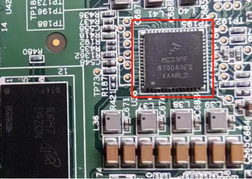
Introduction
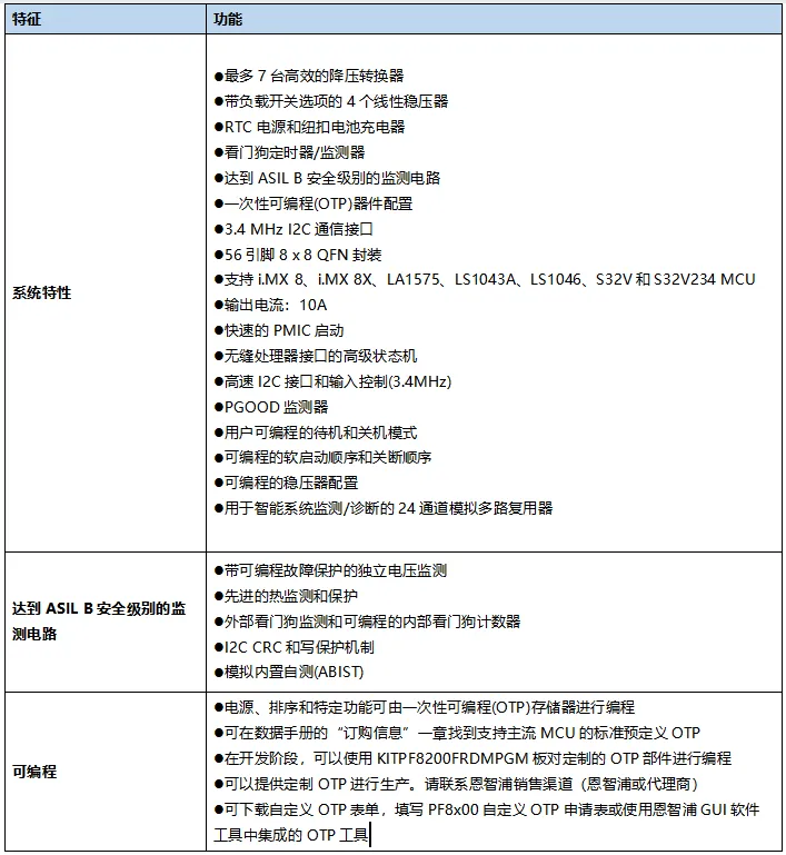
The PF81/PF82 PMIC series is designed for high-performance processing applications such as infotainment, vehicle information services, dashboards, automotive networks, ADAS, and sensor fusion.
Two versions are provided to meet different market needs:
-
PF82 with functional safety, compliant with ISO 26262 standards, provides a robust and flexible solution for ASIL-B (D) automotive applications.
-
PF81 is the basic version of this product, featuring power management and digital control functions without functional safety, suitable for systems not requiring compliance with ASIL-B standards.
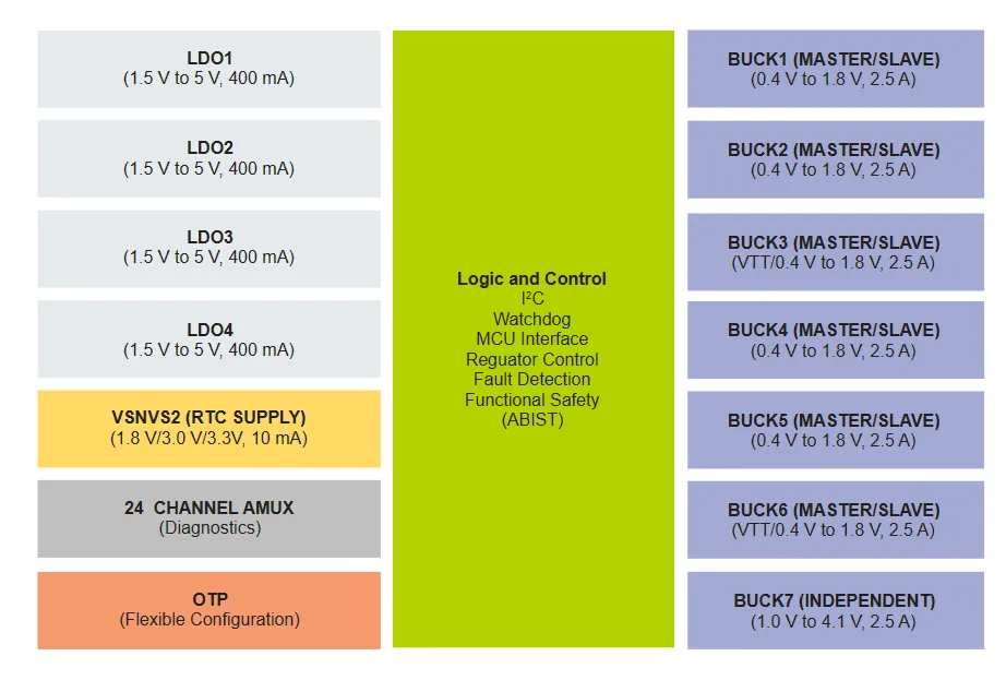
Block Diagram of 8100A0ES
Features
10.2. 355584
①. Introduction
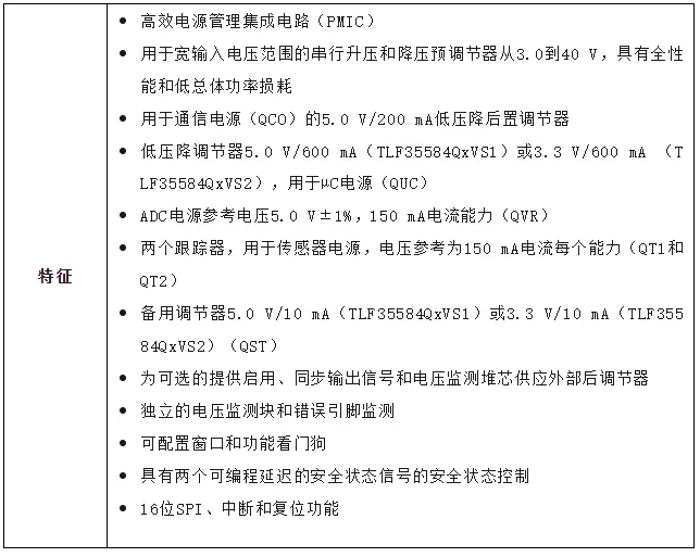
TLF35584 is a multi-output system power supply designed for safety-related applications, providing efficient and flexible front/back regulator concepts across a wide input voltage range for 5V-μC, transceivers, and sensors. Due to its wide switching frequency range, it can optimize efficiency and minimize the use of small filter components. A dedicated reference regulator powers the ADC, providing a step independent of the μC load and can serve as a tracking source for two independent sensor power supplies. Flexible state machine, including wake-up concepts with timers, and backup regulators help users choose among numerous applications.
②. Features
10.3. MPF5024AMMA0ES
The power management chip MPF5024AMMA0ES
Introduction
PF5024 integrates multiple high-performance buck regulators. It can operate as a stand-alone load regulator IC or as a supporting chip for a larger PMIC.
It features one-time programmable (OTP) memory for storing critical startup configurations, significantly reducing the external components typically used to set output voltage and regulator sequences. Regulator parameters can be adjusted via high-speed I2C after startup for flexibility across different system states.
PF5024 is a power management integrated circuit (PMIC) designed for building blocks for main power management of NXP’s high-end multimedia application processors i.MX8 and S32V series. It can also provide power solutions for high-end i.MX6 series and several non-NXP processors.
Features
-
Buck Regulators
–SW1 to SW4: 0.4 V to 1.8 V; 2500mA
–Dynamic Voltage Scaling
–Configurable as multi-phase regulators
–VTT termination mode on SW2
–Programmable current limit
–Spread spectrum and manual tuning of switching frequency
-
PGOOD Output and Monitor
–Global PGOOD output and PGOOD monitor
–Independent PGOOD output for each regulator
-
Independent Enable Input for Each Regulator
-
Clock synchronization via configurable input/output sync pins
-
System Functionality
–PMIC fast startup
–Advanced state machine for seamless processor interface
–High-speed I2C interface support (up to 3.4 MHz)
–User programmable standby and shutdown modes
–Programmable soft-start and power-down sequences
–Programmable regulator configuration
-
OTP (One-Time Programmable) Memory for Device Configuration
-
Monitoring circuit compliant with ASIL B safety level
–Independent voltage monitoring with programmable fault protection
–Advanced thermal monitoring and protection
–External watchdog monitoring and programmable internal watchdog counter
–I2C CRC and write protection mechanisms
–Analog built-in self-test (ABIST)
It is understood that this power chip has been discontinued.
|
Model |
Price |
|
Horizon J3 * 3 |
1000 |
|
TC397 * 1 |
150 |
|
eMMC * 3 |
75 |
|
DDR4 * 3 |
240 |
|
Flash * 3 |
105 |
|
GNSS * 1 |
750 |
|
Switch * 1 |
90 |
|
Ethernet * 1 |
18 |
|
Deserializer |
85+40 |
|
Serializer |
40 |
|
Power Supply |
50+30+40 |
The total estimated cost is approximately 3000 yuan.