
SAIC Roewe’s third generation RX5 is the first fuel vehicle in China equipped with NGP intelligent navigation auxiliary driving function. It was launched in early August 2022 with NGP intelligent driving function. Today, we will decode the design scheme of SAIC Roewe RX5 NGP intelligent driving version domain controller.
This Article Directory
|
1 Roewe RX5 Intelligent Driving Program Overview |
2.3 Core IC Introduction |
|
2 Roewe RX5 Intelligent Driving Domain Controller Scheme |
2.3.1 SOC |
|
2.1 System Architecture |
2.3.2 MCU |
|
2.1.1 System Block Diagram |
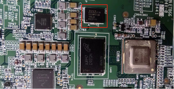
2.3.3 Storage Chip |
|
2.1.2 Core IC List |
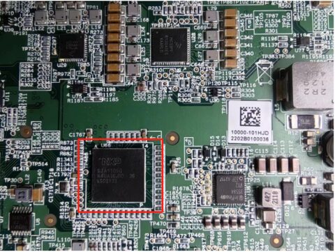
2.3.4 Ethernet/Switch |
|
2.2 Hardware Structure |
2.3.5 Serializer/Deserializer Chip |
|
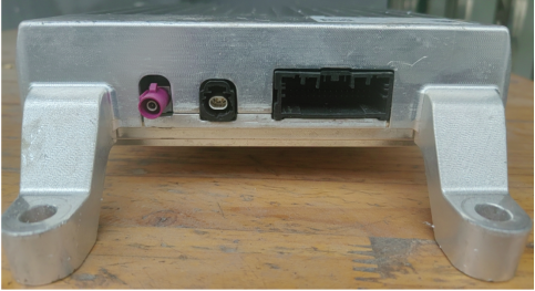
2.2.1 Appearance Structure |
2.3.6 Power Related Chips |
|
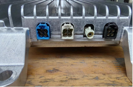
2.2.2 Interface Layout |
3 Roewe RX5 Domain Controller Cost Estimation |
|
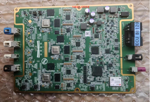
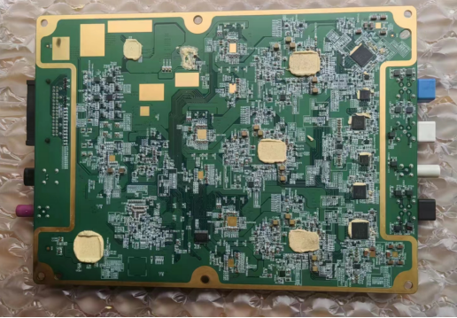
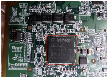
2.2.3 PCB |

To enhance users’ experience of advanced intelligent auxiliary driving functions, SAIC Roewe has invested significant effort in the vehicle’s perception sensor scheme. The all-new third-generation Roewe RX5 NGP intelligent driving version adopts a multi-dimensional perception fusion scheme, equipped with 1 8-megapixel 120° front-view camera, 5 2-megapixel 100° surround-view cameras, 4 360° panoramic cameras, 3 millimeter-wave radars, 12 ultrasonic radars, and high-precision positioning modules, totaling 28 sensors, providing comprehensive coverage of the vehicle’s surrounding environment, enabling the vehicle to have a longer detection distance, a wider detection range, and more accurate identification of more objects.
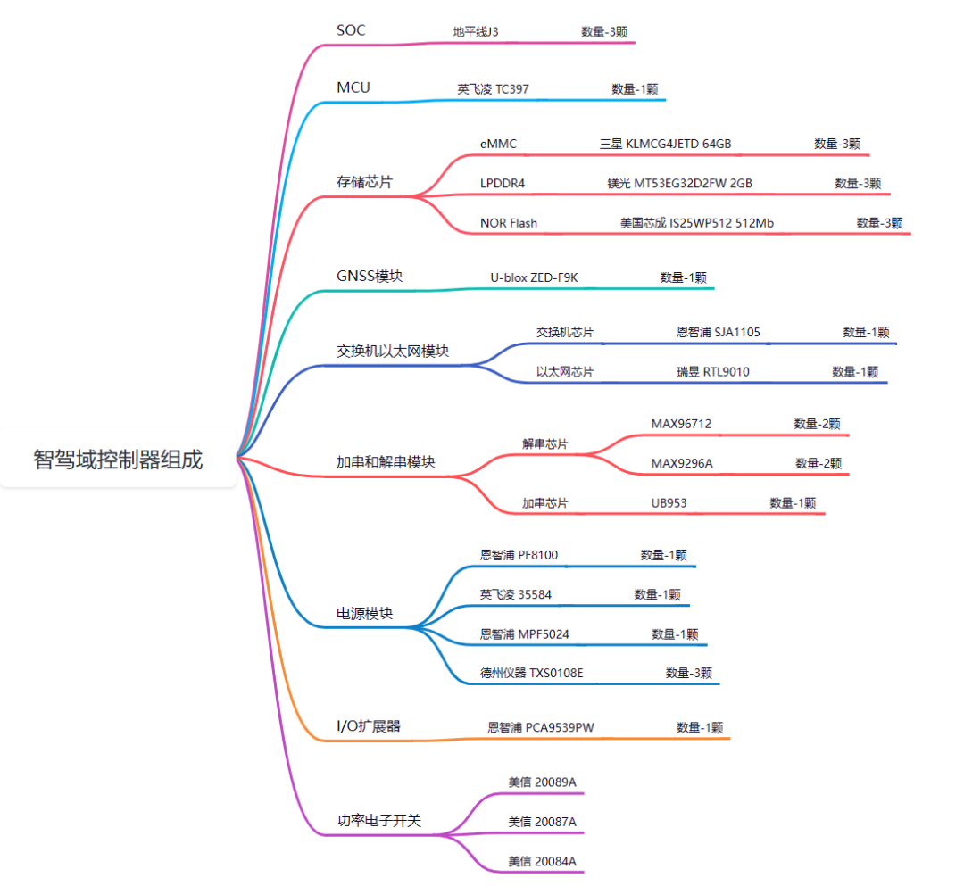
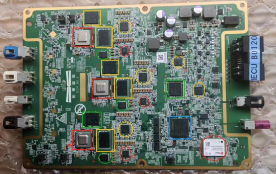
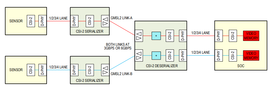
To achieve multi-sensor fusion and more complex algorithms, the SAIC Roewe NGP intelligent driving version domain controller is provided by Hongjing Intelligent Driving. This intelligent driving domain controller uses 3 high-performance domestic AI chips from Horizon Journey 3, which utilize Horizon’s self-developed Bernoulli 2.0 BPU® architecture, achieving various intelligent driving algorithm modules such as environmental perception, map positioning, and fusion planning, enabling 360° surround vision perception coverage. Furthermore, this system supports efficient intelligent driving planning and decision-making algorithms, has deep learning capabilities, and provides iterative updates and other functions.
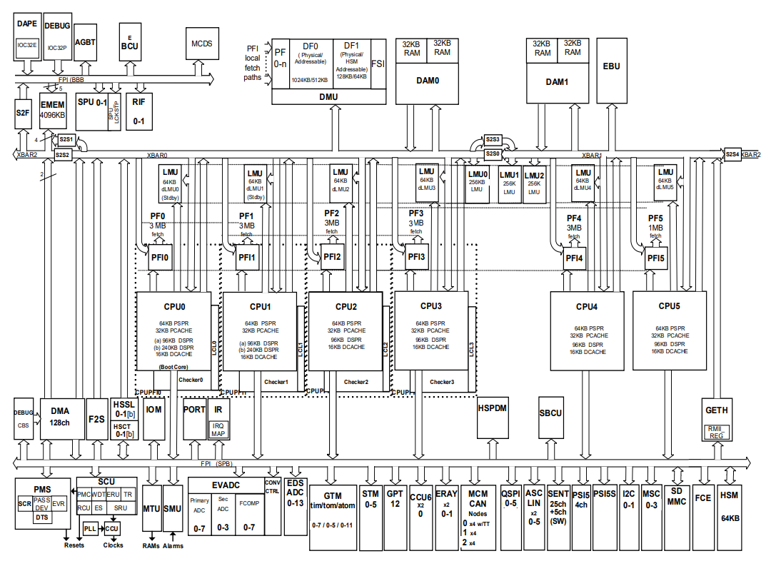
2.1.1 System Block Diagram
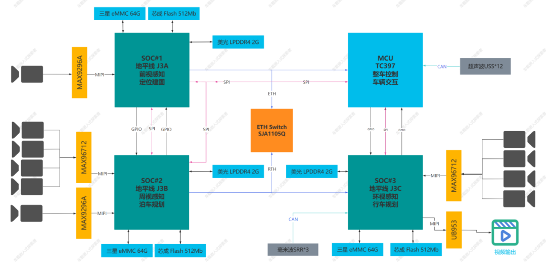
Intelligent Driving Domain Control Composition Diagram
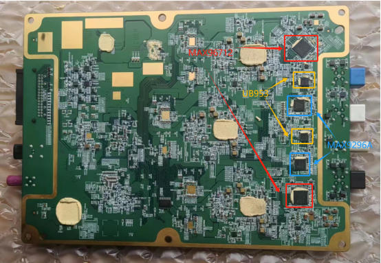
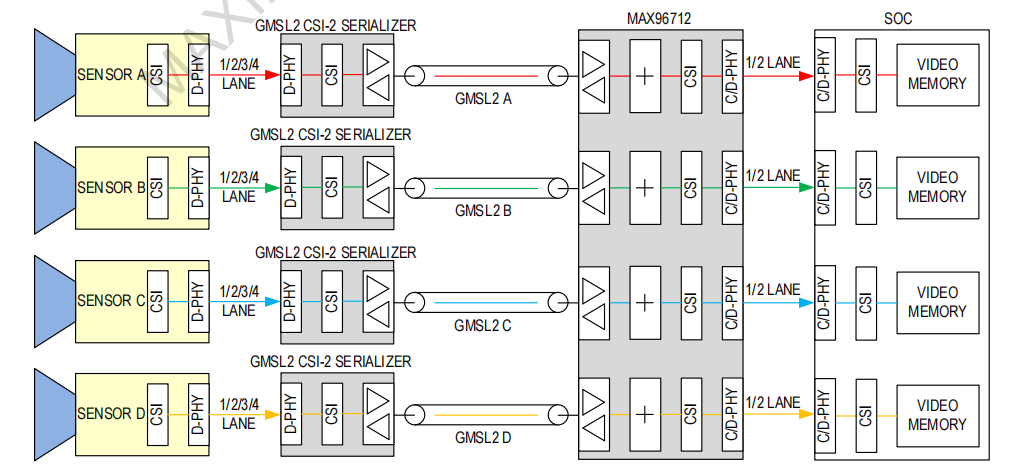
In the diagram, the numbers are as follows:Maxim GMSL MAX96712, Texas Instruments FDLink UB953, Maxim GMSL MAX9296A.
|
|
|
|
|
|
|
|
|
|
|
|
-
Manufactured using TSMC’s 16nm FFC process; -
Using FCBGA484 package, pin pitch of 0.65mm, chip size of 15mmx15mm; -
Complies with automotive AEC-Q100 Grade 2 standards (operating temperature: -40~105 degrees Celsius)
-
Uses 4 Arm Cortex A53 cores, with 32KB/32KB L1 I/D core 512KB Level 2 cache; -
Maximum operating frequency: 1.2GHz; -
Supports Dynamic Frequency Scaling (DFS);
-
Composed of BPU0 core and BPU1 dual-core Bernoulli architecture, computing power of 5TOPS; -
Maximum operating frequency: 950MHz; -
Supports Dynamic Frequency Scaling (DFS);
-
Supports x32 external DDR4/LPDDR4/LPDDR4X DRAM, with a maximum capacity of 4GB;
-
The maximum speed supported by DDR4 can reach DDR4-3200 MT/s;
-
The maximum speed supported by LPDDR4/LPDDR4X can reach 3200MT/s;
-
Supports one Gigabit network interface; -
External Ethernet PHY supports RMII and RGMII protocols; -
Supports Time-Sensitive Networking (TSN) and Audio-Video (AV) traffic;
-
Uses BIF-SPI slave interface, AP SPI master device transmission rate can reach up to 66 MHz;
-
Suitable for AP eMMC master transmission mode, can reach up to 8 lines using BIF-SD device interface HS200 mode (maximum 192MB/s). The application processor (AP) uses BIF-SPI and BIF-SD master interfaces to access J3’s DDR, SRAM, and module registers for data exchange and control;
-
Supports USB3.0 host/device dual-role high-speed interface.
2.3.1.4 Horizon Journey 3 Toolchain
-
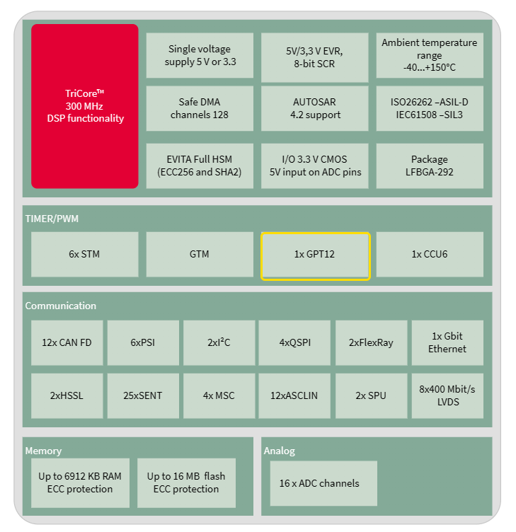
Core: 6 TriCore™ running at 300 MHz (with 4 lock-step cores providing 4000 DMIPS) -
Flash: 16 MB Flash/ECC protection -
RAM: Up to 6.9 MB SRAM/ECC protection -
PHY: 1 Gbit Ethernet -
Peripherals: 12xCAN FD, 2xFlexRay, 12xLINs, 4xQSP, 2xI²C, 25xSENT, 6xPSI, 2xHSSL, 4xMSC, 1x eMMC/SDIO -
LVDS: 8×400 Mbit/s LVDS radar interface -
SPU: 2x SPU (Signal Processing Unit) for radar signal processing -
Timers: Redundant and diverse timer modules (GTM, CCU6, GPT12) -
Encryption: EVITA complete HSM (ECC256 and SHA2) -
Package: BGA-292 package -
Functional Safety: Developed and documented according to ISO 26262/IEC61508, to support safety requirements up to ASIL-D/SIL3 -
AUTOSAR: AUTOSAR 4.2 support -
Power Supply: Single voltage power supply 5 V or 3.3 V -
Temperature: 165°C junction temperature
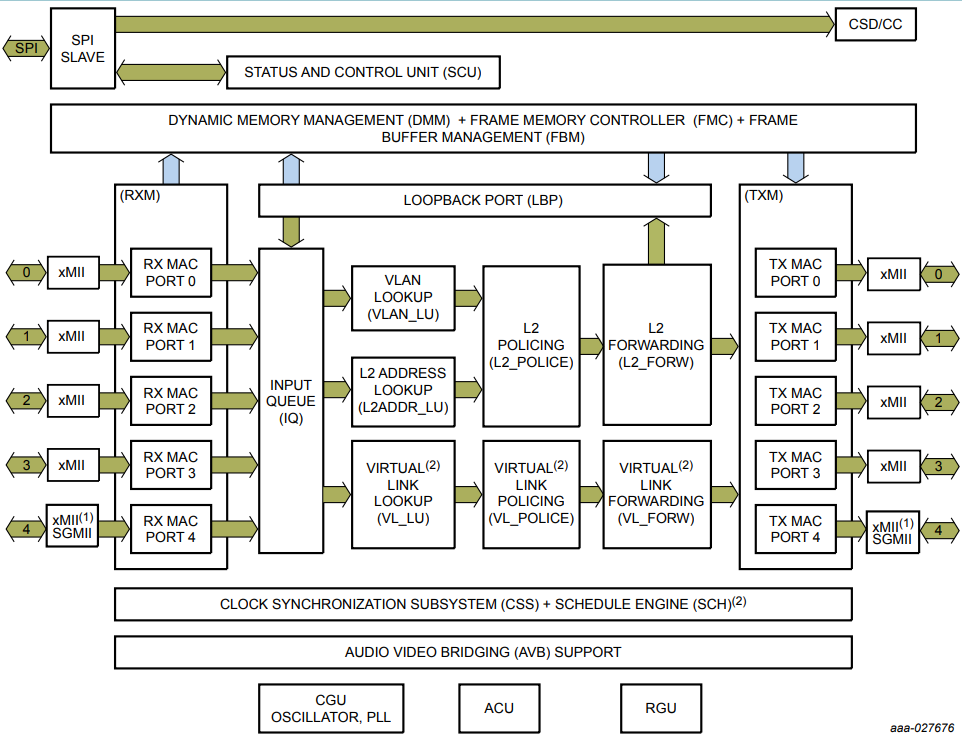
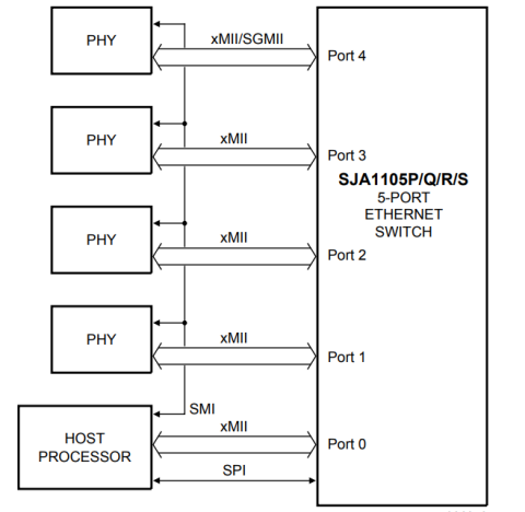
SJA1105 Block Diagram
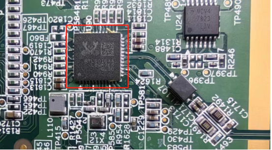
2.3.4.2.2 RTL9010AA Features
-
Wide operating voltage range: 2.5V to 5.5V
-
Low-noise RF applications
-
No noise bypass capacitor required
-
Fast response in line/load transients
-
TTL logic controlled shutdown input
-
Low temperature coefficient
-
300mA LDO output
-
High accuracy ±2%
-
Short-circuit protection
-
Over-temperature protection
-
Current limit protection
-
Short-circuit thermal foldback protection
-
Small TSOT-23-6 package
-
RoHS compliant, 100% lead-free
2.3.5 Serializer/Deserializer Chips
2.3.5.1 MAX96712
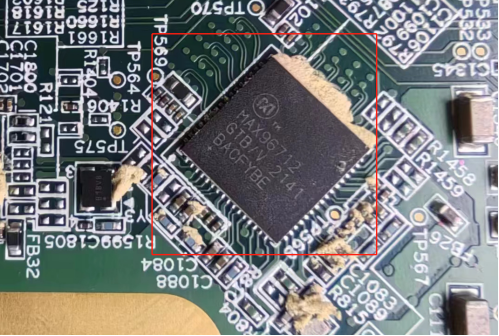
-
MIPI CSI-2 v1.3 output configurable to 2×4 channels, 1×4 lane + 2×2 lanes, or 4×2 lanes
-
Optional D-PHY v1.2, 80Mbps to 2.5Gbps/channel or C-PHY v1.0, 182Mbps to 5.7Gbps/channel -
16/32 channel virtual channel support (D/C-PHY) -
Flexible aggregation and routing of incoming data via CSI-2 VC or frame-level cascading -
Data can be copied and routed to any CSI port -
Supports RAW8/10/12/14/16/20, RGB565/666/888, YUV422 8/10 bit formats -
Dual pixel mode for improved transmission efficiency -
CSI-2 lane reallocation and polarity inversion -
MIPI/GMSL video PRBS generator and checker -
Checkerboard/color gradient pattern generator -
Raw CSI-2 PRBS generator -
Independently configurable all video paths and GMSL/CSI-2 ports
-
Four GMSL inputs with independently configurable GMSL1/2 operation, link speed, and video format
-
Mixed support for GMSL1/GMSL2 and 3G/6G -
Backward compatible with GMSL1 serializers -
GMSL1 forward link speed up to 3.12Gbps -
GMSL2 link speeds of 3Gbps or 6Gbps (forward) and 187.5Mbps (reverse) -
Supports precise synchronization of multiple serializer systems for large camera systems -
GMSL PRBS generator/checker for link testing -
Eye monitor for continuous diagnostics -
Adaptive equalization for up to 15 meters of coaxial cable with multiple inline connectors -
Compatible with 50Ω coaxial cables or 100Ω STP
-
ASIL-B compliant (GMSL2)
-
Video watermark insertion and detection
-
16-bit CRC protection for control channel data that retransmits upon error detection
-
Optional 32-bit CRC protection for video line data
-
ECC protection for video data memory
-
CRC protection for CSI-2 data stream
-
Concurrent control channels for device configuration and communication with remote peripherals
-
3 I2C/UART, 2 SPI, 17 GPIO -
Eight hardware selectable device addresses
-
Programmable spread spectrum to reduce EMI -
64-lead 9mm x 9mm TQFN with exposed pads
2.3.5.2 MAX9296A
MAX9296A deserializer converts single or dual serial inputs to MIPI CSI-2 output. This device operates in GMSL1 or GMSL2 mode. MAX9296A also transmits and receives side-channel data, achieving full-duplex transmission of forward path video and bi-directional control data, at a cost of 50Ω coaxial cables or 100Ω STP cables that comply with GMSL2 or GMSL1 channel specifications.
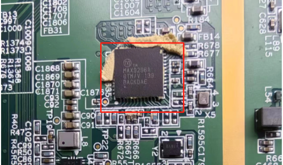
MAX9296A Physical Diagram
MAX9296A Two Independently Operating Video Source Block Diagram
2.3.5.3 UB953
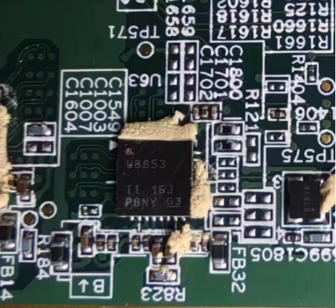
2.3.5.3.1 UB953 Introduction
DS90UB953-Q1 serializer belongs to the TI FPD-Link III device series, designed to support high-speed raw data sensors, including 2.3MP/60fps imagers and 4MP/30fps cameras, satellite radar, lidar, and time-of-flight (ToF) sensors. This chip provides 4.16Gbps forward channel and ultra-low latency 50Mbps bi-directional control channel, and supports power over coaxial (PoC) or STP cables.
-
Complies with AEC-Q100 standard for automotive applications: – Device temperature level 2: environmental operating temperature range of -40°C to +105°C; -
Complies with ISO 10605 and IEC 61000-4-2 ESD standards; -
Coaxial cable powered (PoC) compatible transceiver; -
4.16Gbps grade serializer supports high-speed sensors, including Full HD 1080p 2.3MP 60fps and 4MP 30fps imagers; -
System interface compliant with D-PHY v1.2 and CSI-2 v1.3 standards – up to 4 data channels, with a rate of 832Mbps per channel – supports up to four virtual channels -
Precision multi-camera clock and synchronization -
Flexible programmable output clock generator -
Advanced data protection and diagnostics, including CRC data protection, sensor data integrity checks, I2C write protection, voltage and temperature measurements, programmable alarms, and line fault detection -
Supports single-ended coaxial or shielded twisted pair (STP) cables -
Ultra-low power consumption (0.28W typical) -
Provides functional safety – documentation to assist in ISO 26262 system design -
Wide temperature range: -40°C to 105°C -
Small 5mm × 5mm VQFN package and PoC solution size, suitable for compact camera module designs
2.3.6 Power Related Chips
2.3.6.1 MC33PF 8100A0ES
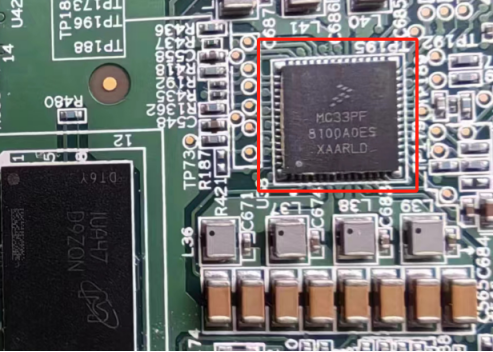
Two versions are offered to meet different market needs:
-
PF82 with functional safety, compliant with ISO 26262 standards, providing a powerful and flexible solution for ASIL-B (D) automotive applications. -
PF81 is the basic version of this product, with power management and digital control functions, without functional safety, suitable for systems that do not require compliance with ASIL-B specifications.
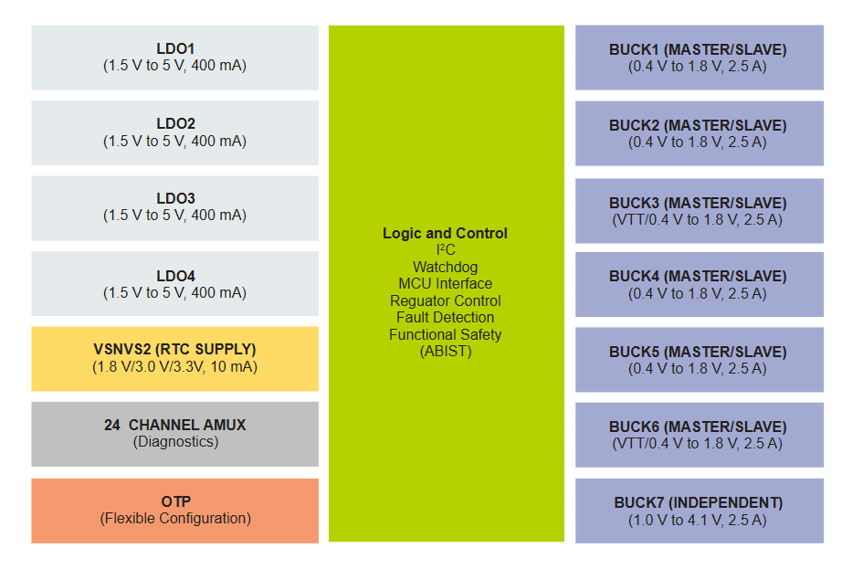
8100A0ES Block Diagram
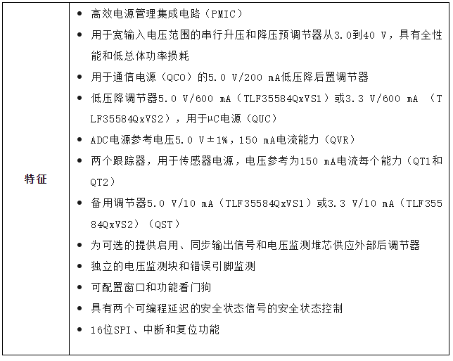
-
Buck Regulators
-
SW1 to SW4: 0.4 V to 1.8 V; 2500 mA
-
Dynamic voltage scaling
-
Configurable as multi-phase regulators
-
VTT termination mode on SW2
-
Programmable current limit
-
Spread spectrum of switching frequency and manual tuning
-
PGOOD output and monitor
-
Global PGOOD output and PGOOD monitor
-
Independent PGOOD output for each regulator
-
Independent enable input for each regulator -
Clock synchronization via configurable input/output sync pins -
System Features
-
PMIC fast startup
-
Advanced state machine for seamless processor interface
-
High-speed I2C interface support (up to 3.4 MHz)
-
User-configurable standby and shutdown modes
-
Programmable soft start sequence and power-off sequence
-
Programmable regulator configuration
-
OTP (One-Time Programmable) memory for device configuration -
Monitoring circuits compliant with ASIL B safety level
-
Independent voltage monitoring with programmable fault protection
-
Advanced thermal monitoring and protection
-
External watchdog monitoring and programmable internal watchdog counter
-
I2C CRC and write protection mechanism
-
Analog built-in self-test (ABIST)
|
|
|
|
|
|
|
|
|
|
|
|
|
|
|
|
|
|
|
|
|
|
|
|
|
|
|
|
|
|
|
|
|
|
|
50+30+40 |
<- Contact & Statement ->


[Statement] Unless otherwise stated in the text, all articles written or reprinted in this public account are intended for learning and exchange purposes, and are not for commercial use. They do not represent the views and positions of this account. All information and images quoted in this public account are organized or quoted by the individual public account ADS Think Tank Liu Er based on official or public information. The copyright of the quoted and reprinted content in this public account belongs to the original author. For any copyright or other issues, please contact Liu Er (WeChat ID: adas_miao), and this account will handle it promptly.