Decades ago, when embedded system designers wanted to reduce costs, they would use the PC architecture that was mass-produced at that time. By adopting hardware and software originally developed for PC architecture, embedded system designers could achieve high reliability components validated by tens of millions of consumer electronics applications while reducing development costs. The PC bus provided a highly attractive low-cost alternative for dedicated embedded applications. In addition to these advantages, embedded developers could also take full advantage of easy-to-use design tools and open-source operating systems based on familiar architectures. By migrating designs to PC architecture, designers could pass on low costs to end consumers and shorten development cycles.
The era of PCs is long gone. The PC architecture can no longer provide the mass production advantages it once did. Today, embedded system developers are considering how to leverage the cost advantages brought by mass production in the consumer electronics market, with the smartphone market becoming the first choice. The number of smartphones sold worldwide each year reaches billions, and design engineers in various fields are trying to fully utilize the high performance and low cost advantages of key components in today’s mobile solutions. Just like the role PC architecture played twenty years ago, the mobile market provides engineers with familiar hardware architectures and applications, whose performance has been validated in the fiercely competitive consumer electronics market.

The development of current portable device design is driven by the interfaces and buses defined by the MIPI Alliance. Founded in 2003, the MIPI Alliance aims to establish a comprehensive set of specifications for mobile and mobile-related devices. The goal of the Alliance is to provide the hardware and software interface specifications that device vendors need to create innovative mobile products while accelerating time-to-market and reducing costs. By establishing a complete set of core standards, the MIPI Alliance enables mobile device manufacturers to source components from different suppliers and easily optimize design performance.
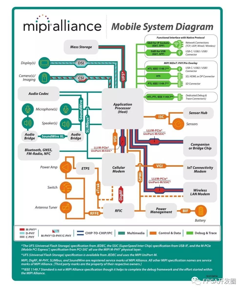
Figure 1. The MIPI Alliance has established a set of core standards to simplify mobile system design and ensure interoperability (Image from MIPI Alliance)
The organization has grown from its initial four members to now hundreds of members, and its reputation in the smartphone industry is well-known. All major chip manufacturers use the specifications set by the MIPI Alliance, and every smartphone uses at least one MIPI specification.

In fact, the influence of the MIPI Alliance has far exceeded the scope of the mobile industry. As mobile interconnects integrate into all aspects of people’s lives, more and more design engineers from different industries are trying to adopt mobile technology for their designs. However, they also face numerous obstacles in this process. Many cameras and displays used in embedded systems do not match the type or number of interfaces on today’s mobile application processors (AP).
Application processors, image sensors, and displays may be the MIPI standard components from which embedded system designers can benefit the most. Today’s mobile system designs often include displays using MIPI Display Serial Interface (DSI) and image sensors using MIPI Camera Serial Interface (CSI-2). Both DSI and CSI-2 interfaces are based on the D-PHY physical layer bus protocol. D-PHY uses a differential clock and 1-4 pairs of differential data lines to transmit data, and D-PHY is a center-aligned source-synchronous interface that transmits data on both the rising and falling edges of the clock. One of the unique features of D-PHY is its ability to “instantaneously” convert differential signals to single-ended signals.
When using traditional or dedicated displays and traditional or dedicated image sensors in designs, how can embedded design engineers leverage the numerous advantages offered by the MIPI market? Take the industrial market as an example. Embedded application design engineers have long relied on displays with LVDS, RGB, or SPI interfaces. However, most embedded processors do not have DSI interfaces. Industrial application design engineers who want to take advantage of MIPI processors and application advantages while retaining traditional LVDS displays need to bridge the LVDS displays with MIPI-compliant application processors. One solution to this problem is to build a video bridging solution from OpenDSI, LVDS, or dedicated interfaces to MIPI DSI (see Figure 2).
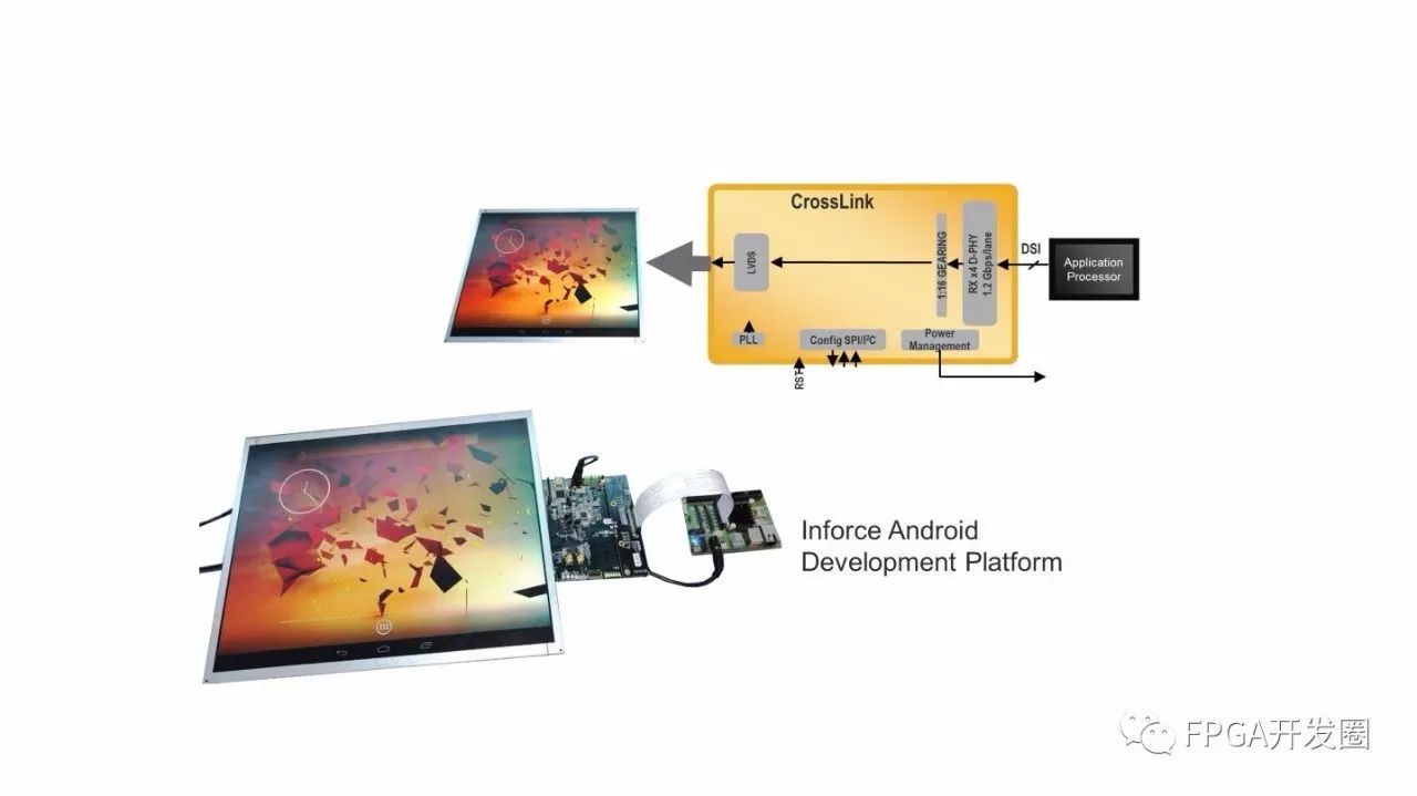
Figure 2. The video bridging solution enables design engineers to interconnect traditional displays with MIPI application processors
Similarly, many design engineers in the industrial sector also want to retain CMOS cameras in their designs while adopting the latest generation of mobile processors and applications. Figure 3 (below) illustrates how to bridge traditional CMOS parallel output with MIPI application processor CSI-2 input.
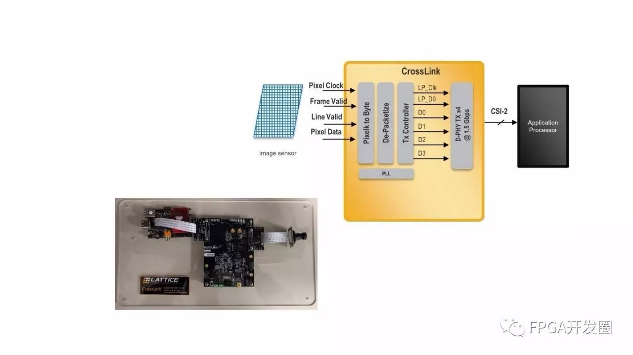
Figure 3. In this example, the video bridging solution enables development engineers to interconnect traditional image sensors with MIPI application processors
In the automotive industry, the use of MIPI-compliant application processors and components is also increasing. As applications in automotive design, such as Advanced Driver Assistance Systems (ADAS) and in-vehicle infotainment systems, require more content to be displayed and an increasing number of cameras, the demand for video bridging solutions is also growing. With the help of cameras, drivers can not only see vehicles behind them when reversing, but they can also replace side mirrors to provide 360-degree visibility and support various applications such as lane change tracking and blind spot reduction. In today’s vehicles, design engineers can aggregate video data from multiple image sensors, stitch it together, and transmit it to the application processor through a single CSI-2 interface.
Design engineers find that video bridging solutions that aggregate data from multiple cameras or output it separately to multiple displays are very useful in gaming applications. For example, one of the latest trends in the rapidly developing virtual reality (VR) market is transitioning from a single display to dual display headsets that each use half the bandwidth to provide users with stereoscopic images. But if the application processor only has one DSI interface, how can design engineers split the video output to two displays? Figure 4 (below) illustrates how to use a video bridging solution to split a single DSI video data output from the application processor into two outputs for the left and right displays. This bridge can support two HD or one QHD display with an I/O rate of up to 1.5 Gbps/channel.
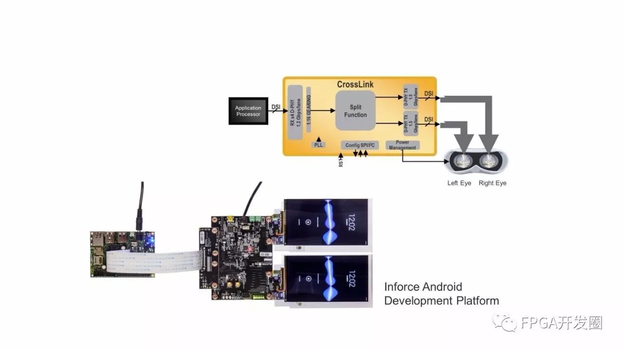
Figure 4. This bridging solution splits video data into two DSI outputs to support stereoscopic images in VR headsets
Another potential bridging application is to aggregate data into a single CSI-2 output. Figure 5 (below) illustrates how drone or VR developers can use new bridging devices to aggregate the video outputs from multiple image sensors into a single input that meets the application processor interface requirements. This bridge can be used in cases where the application processor in the design cannot provide enough interfaces to support image sensor inputs, or where there is processing latency between image sensors and imaging data. In this case, the processor must receive multiple CSI-2 outputs with minimal latency simultaneously. The multiple merged video streams must also share a common clock, and in some cases, a separate power-up timing may be required.
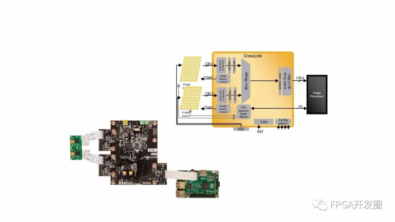
Figure 5. Drone and other system manufacturers integrate multiple CSI-2 cameras in their designs, so they may need to merge video content for delivery to the application processor for processing

To meet the demands of new video applications, today’s embedded video application design engineers need high-performance, low-power, small-size bridging solutions. An ideal bridging solution should be able to convert incompatible interfaces for cameras, displays, and application processors, aggregate multiple video streams into a single output, or split a single video output into multiple.
One way to solve this problem is to use a universal multi-channel passive switch to route signals to multiple locations on the circuit board. However, most multiplexing/demultiplexing solutions do not provide the high performance or high level of design flexibility that design engineers require. Another option is to invest in Application-Specific Standard Products (ASSP) or Application-Specific Integrated Circuits (ASIC)-based bridging solutions. Most bridging solutions have a narrow application scope, and the high one-time engineering costs (NRE) and long development cycles make this approach unfeasible.
Lattice Semiconductor’s CrossLink FPGA has been on the market for over a year, providing design engineers with design flexibility and accelerating time-to-market. It is the industry’s fastest MIPI D-PHY bridging device, capable of transmitting 4K ultra-high-definition video at a bandwidth of 12 Gbps. CrossLink devices are designed to address interface mismatches between application processors, image sensors, and displays, enabling low-cost, highly compact bridging solutions that support various leading and existing protocols.
CrossLink bridging devices feature two MIPI D-PHY hard cores and a mobile application-oriented FPGA architecture that supports multiplexing, aggregation, demultiplexing, arbitration, splitting, and data conversion functions. Each MIPI D-PHY block in the device supports up to four data channels and one clock channel for transmitting and receiving (Tx and Rx) data. Two programmable I/O banks support multiple interfaces, including MIPI D-PHY, MIPI CSI-2, MIPI DSI, CMOS, RGB, SubLVDS, SLVS, LVDS, and Open LDI.
The FPGA architecture in the device includes 5936 4-input LUTs, 180 kbit RAM blocks, and 47 kbit distributed RAM. These LUTs are located next to dedicated registers in programmable function units (PFU) and serve as fundamental building blocks for logic operations, RAM, and ROM functions. A programmable interconnect network connects each PFU block. Programmable I/O banks, embedded I2C, embedded MIPI D-PHY, and embedded RAM (EBR) blocks are distributed among the PFUs. Design engineers can configure the PFU modules using Lattice Diamond design software to implement their designs.

The development process for interface bridging solutions based on CrossLink devices is relatively straightforward. Developers first select the IP they want to use or generate from the IP configuration tool Clarity Designer in Lattice Diamond FPGA design software. Clarity Designer supports configuring multiple IPs, building interconnections between IPs, and planning the resources used by the IPs in the design.
Once the IP is generated, development engineers can simulate it using the Aldec simulator. Engineers only need to open the Aldec simulator, open the tool, and click execute. After the simulation is complete, engineers can review the simulation results. Hardware debugging can be performed using Lattice’s Reveal on-chip debugging tool. The Reveal tool is integrated into Lattice Diamond FPGA design software, featuring one-click operation, advanced triggering capabilities, a simple workflow, support for modifying the original design, and enhanced logic analyzer waveform display capabilities.
To accelerate system development, Lattice also provides the CrossLink LIF-MD6000 master control connection evaluation board. This evaluation board includes a CrossLink-MD6000 device in an 81-ball csfBGA package. In addition, the evaluation board features a Mini USB Type-B connector to FTDI and circuitry connecting FTDI to CrossLink via SPI interface. The kit also includes two interface boards.

Twenty years ago, the dominant PC architecture drove the development of various markets. Today, the rapidly evolving mobile market is having a similar impact on industries such as industrial, automotive, and medical. As mobile technology continues to expand into new application areas, design engineers of mobile-related products can leverage the mass production advantages of the mobile market and the cost and performance advantages of mobile processors, displays, and image processors with the help of bridging solutions.

FPGA deep learning applications accelerate again; Deep Insight Technology launches a multi-scenario artificial intelligence service solution based on Xilinx
The electronic engineering genius has such a mysterious tool in their pocket
PON: The evolution of data transmission to homes
Huawei Cloud releases FACS FP1 OpenCL instance in collaboration with Xilinx at XDF
The secret weapon of the Sidewinder-100 PCIe NVMe Controller
One thousand ways to play with drones; if you don’t come to play, you’re out!
A story sparked by a Xilinx packaging box
Open-source tools help you easily implement binarized neural networks on FPGA
Stunned! The data center acceleration artifact—1680-core processor + FPGA!
Supporting multiple high-sampling-rate ADCs: XA-RX module based on Xilinx Artix A200T FPGA
Deep dive: Huawei FPGA accelerates cloud services, disrupting traditional FPGA development
[Expert Q&A] PS eFUSE integrity power-on/power-off sequence requirements
Opal Kelly launches SYZYGY specification interface for FPGA modules
RFSoC starts shipping! Fully accelerating 5G wireless, wired Remote-PHY, and other applications
The eyes of robots need a Spartan-6 FPGA
Z-turn SBC simplified version based on Xilinx Z-7007—Z-turn Lite
[Expert Q&A] Is the Vivado result reproducible for the same tool input?
New member joins the Arty family: Arty S7 development board based on Xilinx Spartan-7 FPGA
Watch a 15-minute video to improve C/C++ code running efficiency?
Super compatibility! Xilinx Zynq 7045 supports 29 types of CMOS sensors with Denali-MC HDR IP
The artifact for debugging hardware bugs—a new type of logic analyzer
FPGA memory recommendations (using Vivado Design Suite)
The 100G era of data centers has arrived! Virtex UltraScale+ FPGA helps speed up core networks!