Click the above  “Easily Learn Electronics” to follow us and easily learn electronic knowledge.
The Inter-Integrated Circuit (I2C) bus is a synchronous serial data communication bus, where communication is initiated by the master device and controlled by the addressed slave devices. Nodes on the I2C bus are easy to connect, requiring only two open-drain signal lines (SDA for data and SCL for clock). The capacitance on these lines is the main factor limiting transmission rate and distance between nodes [1]. To extend the rate and distance, it is necessary to use buffers that can identify data direction. The design case described in this article fully demonstrates the advantages of the PCA9605 buffer.
The PCA9605 is a single-chip CMOS integrated circuit that can implement bus buffering functions in applications including the I2C bus. This buffer can extend the bus load by buffering the SCL and SDA lines, allowing the maximum permissible bus capacitance on both sides of the buffer. In its most basic implementation, this buffer allows an extended number of slave devices to connect to a master device. In this design example, the master device is a PIC microcontroller [2], and the slave devices are two data converters, one being an analog-to-digital converter and the other a digital-to-analog converter. The direction pin (DIR) of the PCA9605 is fixed to ground since the clock is provided by the master device (unidirectional clock mode). Figure 1 shows the overall schematic.
U2 ADC captures the analog signal from the signal generator and converts it into a digital signal, which is then sent to buffer U3, driven by U3 for cable transmission, and continues through relay U4. The SDA data line needs to be bidirectionally driven from U3 to U4 and from U4 to U3. Ultimately, the digitalized signal is produced by U5 ADC. If longer cable transmission is required, another buffer can be inserted in the middle of the circuit for extension. This method can cover wired transmission distances of up to several hundred meters [3].
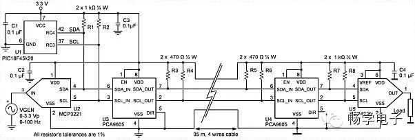
Figure 1: Circuit schematic connecting two nodes with extended I2C bus.
Figure 2 shows the transmission of DAC address (0xC0) over the cable bus at a rate of 125kHz. Channel 1 connects to the bus-side SDA line (pin 6 of U4), where the signal is driven by the buffer to eliminate glitches and capacitive interference from the clock line, as well as the RC effect caused by the open-collector integration and trace capacitance due to pull-up resistors. Channel 2 shows the SDA data signal driven by the buffer (pin 7 of U4), while channel 4 (pin 2 of U4) is the clock SCL after buffering. The clock signal on the cable (pin 3 of U4) is shown in channel 3, and channel 4 is the signal driven by the buffer (pin 2 of U4).
If a unipolar analog signal with a voltage amplitude at full input scale is sent to ADC U2 during system testing, the waveform shown in Figure 3 can be obtained at the output load of DAC U5. This design fully utilizes the characteristics of the ADC and DAC circuits, allowing them to handle rail-to-rail signals. This low-frequency signal can be improved by adding a low-pass filter at the DAC output, as the low-pass filter can reduce sampling and reconstruction noise.
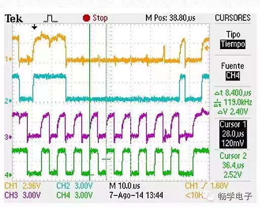
Figure 2: Slave node signals before and after buffering.
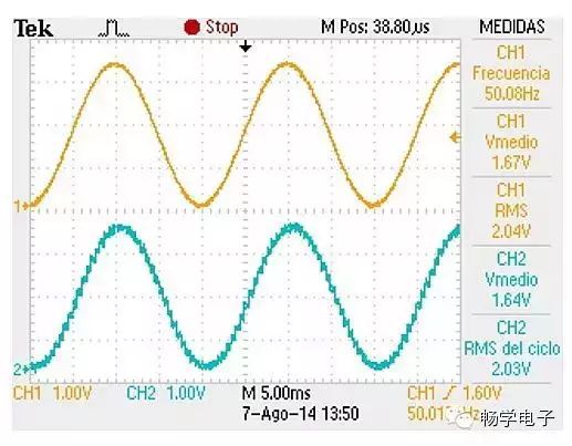
Figure 3: Full-scale input sine wave sent via I2C.
> > > > > > > > > > > > > > > > > > > > > > > > > > > > > > > > > > > > > > > > > > > > > > > > > > > > > >