Siemens Comprehensive + TIA Portal + EPLAN Electrical Drawing Video Recordings are being sold at a low price in a package!
Chuangkong Education Siemens Comprehensive Class Course Introduction

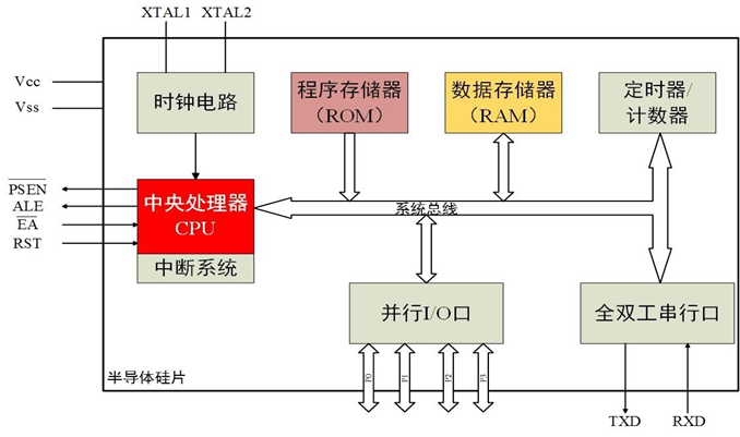
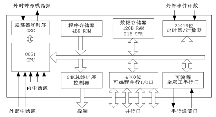
The basic structure of a microcontroller includes six parts: Central Processing Unit (CPU), memory, timer/counter, input/output interface, interrupt control system, and clock circuit.
I. Basic Components
Central Processing Unit (CPU)
Consists of an arithmetic unit and a control unit, which are the core of the microcontroller. The arithmetic unit is used for various calculations, while the control unit coordinates the operation of various parts of the microcontroller.
Used to store programs and raw data.
The clock circuit generates control signals for the microcontroller’s operation, ensuring the microcontroller executes instructions in a strict sequence.
Timer/Counter: Implements timing or counting functions.
Input/Output Interface (I/O): Enables data transfer between the microcontroller and other devices.
Interrupt Control System: Responds to interrupt requests from interrupt sources.
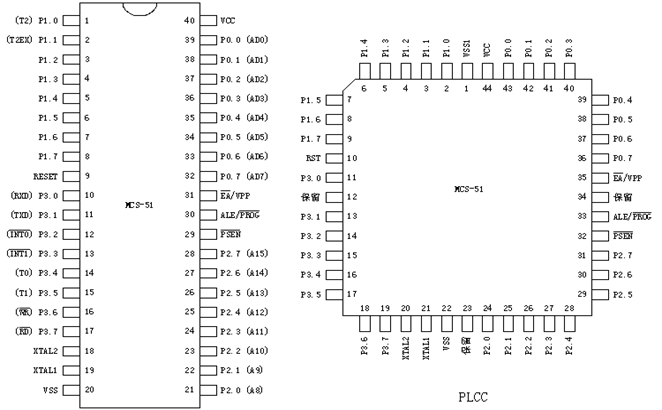
II. Microcontroller Pins
Dual Inline Package (DIP)
Plastic Leaded Chip Carrier (PLCC)
Power Pins: VCC (Pin 40) and VSS (Pin 20) connect to the positive and negative terminals of the power supply, respectively.
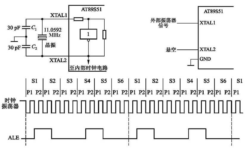
Clock Circuit Pins: The microcontroller requires clock pulse signals to operate, connected via (Pin 18) and (Pin 19) to the oscillator circuit.
The control signal pins include the following four:
EA (Pin 31): When EA is high, it executes the internal ROM program first, and when low, it only executes the external ROM program.
RST (Pin 9): When a high signal lasting more than two machine cycles is input, it resets the microcontroller, initializing it and allowing it to re-execute the program.
ALE (Pin 30): Controls the time-sharing transmission of the lower 8 bits of address and data when accessing external memory and other peripherals.
PSEN (Pin 29): External program memory read enable signal.
There are 32 parallel input/output pins:
PO Pins (Pins 39-32): Can be used as address/data bus ports or as general I/O ports.
P1 Pins (Pins 1-8): Generally only used as I/O ports.
P2 Pins (Pins 21-28): Can output the higher 8 bits of the address when accessing external memory, and can also be used as general I/O ports.
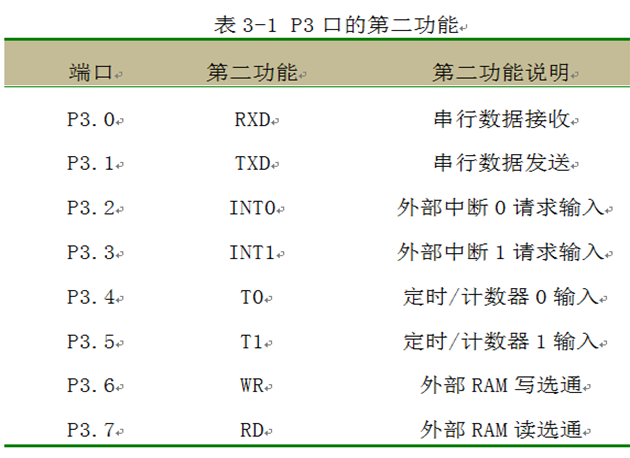
P3 Pins (Pins 10-17): Mainly used for their secondary functions, but can also be used as general I/O ports.
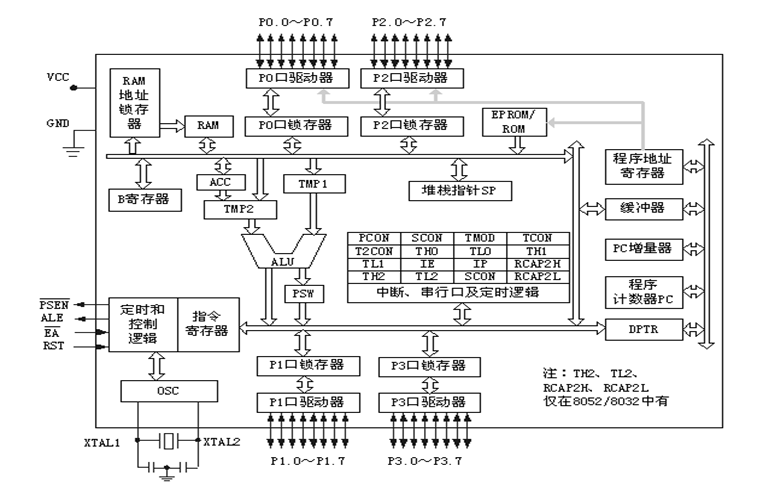
III. Parallel Input/Output
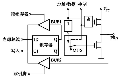
2 Tri-state Data Input Buffers BUF1 and BUF2.
2 Field Effect Transistors (FET).
1 Multiplexer, 1 Inverter, and 1 AND gate.
P0 Pin Working Principle – Used as Multiplexed Address/Data Bus
Output: When the “control” signal is 1, the hardware automatically switches the MUX to the upper position, connecting the output of the inverter, while enabling the AND gate.
① When the output address/data information = 1, the output of the AND gate is 1, the upper field effect transistor is turned on, and the lower field effect transistor is turned off, making P0.x pin output 1.
② When the output address/data information = 0, the upper field effect transistor is turned off, the lower field effect transistor is turned on, making P0.x pin output 0.
P0 Pin Working Principle – Used as Multiplexed Address/Data Bus
Input: When P0 pin is used as data input, it only reads information from the external pins, with the “control” signal being 0, allowing the MUX to connect to the latch Q terminal.
When P0 pin accesses external memory in a multiplexed address/data manner, the CPU automatically writes FFH to P0 pin, turning off the lower field effect transistor, while the upper field effect transistor is also turned off due to the control signal being 0, ensuring high impedance input for the data information, which directly enters the internal bus through the input buffer BUF2 from the external data via P0.x pin.
① When D latch is 1, the terminal is 0, the lower field effect transistor is turned off, and the output is an open-drain, so a pull-up resistor must be connected externally to achieve a high output level;
② When D latch is 0, the lower field effect transistor is turned on, making P0 pin output low level.
P0 Pin Working Principle – Used as General I/O Pin
Input: Two reading methods: “Read Latch” and “Read Pin”.
① When the CPU issues the “Read Latch” command, the latch status is read from the Q terminal via the upper tri-state buffer BUF1 into the internal bus.
② When the CPU issues the “Read Pin” command, the latch output status Q=1 (Q terminal is 0), which makes the lower field effect transistor turn off, and the pin status enters the internal bus via the lower tri-state buffer BUF2.
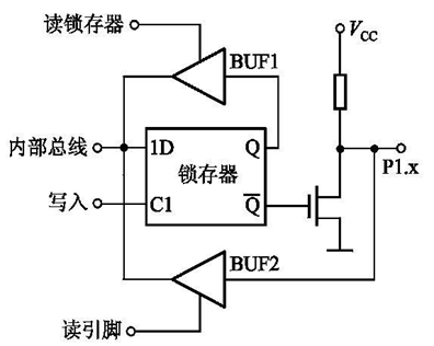
2 Tri-state Data Input Buffers BUF1 and BUF2.
1 Field Effect Transistor (FET) and 1 internal pull-up resistor.
P1 Pin Working Principle – Used only as General I/O Pin
① If the CPU outputs 1, Q=1, Q-=0, the field effect transistor is turned off, and P1.x pin outputs 1;
② If the CPU outputs 0, Q=0, Q- =1, the field effect transistor is turned on, and P1.x pin outputs 0.
P1 Pin Working Principle – Used only as General I/O Pin
Input: Divided into “Read Latch” and “Read Pin”
① When reading the “Latch”, the output Q status enters the internal bus via the input buffer BUF1;
② When “Reading Pin”, write 1 to the latch first, making the field effect transistor turn off, and the voltage level at P1.x pin enters the internal bus via the input buffer BUF2.
2 Tri-state Data Input Buffers BUF1 and BUF2.
1 Field Effect Transistor (FET) and 1 internal pull-up resistor.
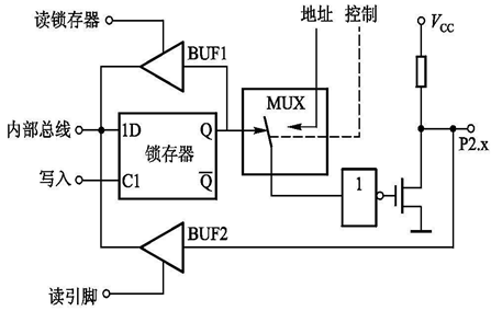
P2 Pin Working Principle – Used as Address Bus
Under the control signal, the MUX connects to the “Address”.
① When the “Address” is 0, the field effect transistor is turned on, and the P2 pin outputs 0;
② When the “Address” line is 1, the field effect transistor is turned off, and the P2 pin outputs 1.
P2 Pin Working Principle – Used as General I/O Pin
Output: Under the internal control signal, the MUX connects to the latch Q terminal.
① When the CPU outputs 1, Q=1, the field effect transistor is turned off, and P2.x pin outputs 1;
② When the CPU outputs 0, Q=0, the field effect transistor is turned on, and P2.x pin outputs 0.
P2 Pin Working Principle – Used as General I/O Pin
Input: Divided into “Read Latch” and “Read Pin” methods.
① When “Reading Latch”, the Q signal enters the internal bus via the input buffer BUF1;
② When “Reading Pin”, write 1 to the latch first, making the field effect transistor turn off, and the voltage level at P2.x pin enters the internal bus via the input buffer BUF2.
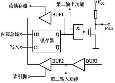
3 Tri-state Data Input Buffers BUF1 and BUF2.
1 Field Effect Transistor (FET) and 1 internal pull-up resistor.
1 Multiplexer (MUX) and 1 NAND gate
P3 Pin Working Principle – Used for Secondary Function
Output: The latch of this bit needs to be set to “1” to enable the NAND gate.
When the second output is 1, the field effect transistor is turned off, and P3.x pin outputs 1;
When the second output is 0, the field effect transistor is turned on, and P3.x pin outputs 0.
P3 Pin Working Principle – Used for Secondary Function
Input: The latch of this bit and the second output function terminal must be set to 1 to ensure the field effect transistor is off; the information of P3.x pin is obtained from the output of input buffer BUF3.
P3 Pin Working Principle – Used as General I/O Pin
Output: The second output function terminal should remain “1”, enabling the NAND gate.
When the CPU outputs 1, Q=1, the field effect transistor is turned off, and P3.x pin outputs 1;
When the CPU outputs 0, Q=0, the field effect transistor is turned on, and P3.x pin outputs 0.
P3 Pin Working Principle – Used as General I/O Pin
Input: The output latch of P3.x pin and the second output function should be set to 1, ensuring the field effect transistor is off.
The information of P3.x pin enters the internal bus via input buffers BUF3 and BUF2, completing the “Read Pin” operation;
It can also perform the “Read Latch” operation, at this time the Q terminal information enters the internal bus via buffer BUF1.
Before reading the pins of the four parallel ports (P0-P3), the latches must be set to “1” to ensure the field effect transistors are off, avoiding interference from the latch data.
Since an additional preparation step of setting to “1” is required before the input operation, it is called a “quasi-bidirectional port”.
All four parallel ports (P0-P3) are quasi-bidirectional ports.
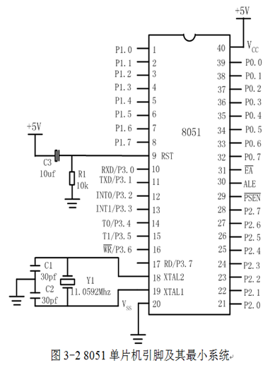
IV. Minimum System Board of the 8051 Microcontroller
The 8051 microcontroller has 4KB of flash memory, making it a minimal application system for digital input/output.
When constructing the minimum application system of the 8051 microcontroller, it only requires an external clock circuit and reset circuit, as shown in the figure below.
Note: This minimum application system can only serve as a small digital measurement and control unit.
(Content sourced from the internet, copyright belongs to the original author)
Disclaimer: If there are copyright issues, please contact for removal!No individual or organization bears any legal responsibility.
Siemens Comprehensive + TIA Portal + EPLAN Electrical Drawing Video Recordings are being sold at a low price in a package!
Chuangkong Education Siemens Comprehensive Class Course Introduction