Source: Semika
Original Author: Semika
Chip manufacturing is one of the most complex processes in the world today. It is a complex process accomplished by numerous top-tier companies. This article aims to summarize this process and provide a comprehensive overview of it.
The semiconductor manufacturing process consists of many steps, reportedly hundreds or even thousands. This is not an exaggeration; a factory with a billion-dollar investment might only handle a small portion of the entire process. Given the complexity of this process, this article will categorize it into five main categories: wafer manufacturing, photolithography and etching, ion implantation, thin film deposition, and packaging and testing.
Semiconductor Manufacturing Process – Wafer Manufacturing
Wafer manufacturing can be divided into the following five main processes:
(1) Crystal Pulling
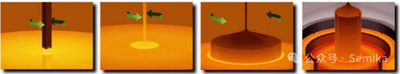
◈ Dopant polycrystalline silicon is melted at 1400 degrees
◈ High-purity argon gas is injected as an inert gas
◈ A single crystal silicon “seed” is placed into the melt and slowly rotated during “pulling”.
◈ The diameter of the single crystal ingot is determined by temperature and extraction speed
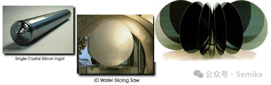
(2) Wafer Slicing
Silicon ingots are sliced into individual wafers using precise “saws”.
(3) Wafer Lapping and Etching
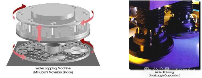
◈ The sliced wafers are mechanically polished using a rotating grinder and alumina slurry to make the wafer surfaces flat and parallel, reducing mechanical defects.
◈ The wafers are then etched in a nitrogen acid/acetic acid solution to remove microcracks or surface damage, followed by a series of high-purity RO/DI water baths.
(4) Wafer Polishing and Cleaning
◈ Next, the wafers are polished through a series of chemical and mechanical polishing processes known as CMP (Chemical Mechanical Polish).
◈ The polishing process usually includes two to three polishing steps, using progressively finer slurries and intermediate cleaning with RO/DI water.
◈ Final cleaning is performed with SC1 solution (ammonia, hydrogen peroxide, and RO/DI water) to remove organic impurities and particles. Then, HF is used to remove native oxides and metallic impurities, and finally SC2 solution allows ultra-clean new native oxides to grow on the surface.
(5) Wafer Epitaxial Processing
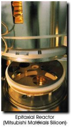
◈ Epitaxial processes (EPI) are used to grow a layer of single crystal silicon from vapor onto a single crystal silicon substrate at high temperatures.
◈ The process of vapor phase growth of single crystal silicon layers is called vapor phase epitaxy (VPE).
SiCl4 + 2H2 ↔ Si + 4HCl
The reaction is reversible, meaning that if HCl is added, silicon will be etched off the surface of the wafer.
Another reaction to generate Si is irreversible:
SiH4 → Si + 2H2 (silane)
◈ The purpose of EPI growth is to form layers with different (usually lower) concentrations of electrically active dopants on the substrate. For example, an N-type layer on a p-type wafer.
◈ About 3% of the wafer thickness.
◈ No contamination for subsequent transistor structures.
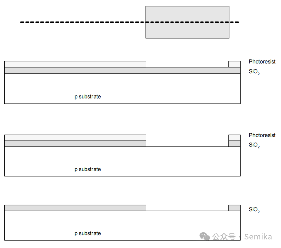
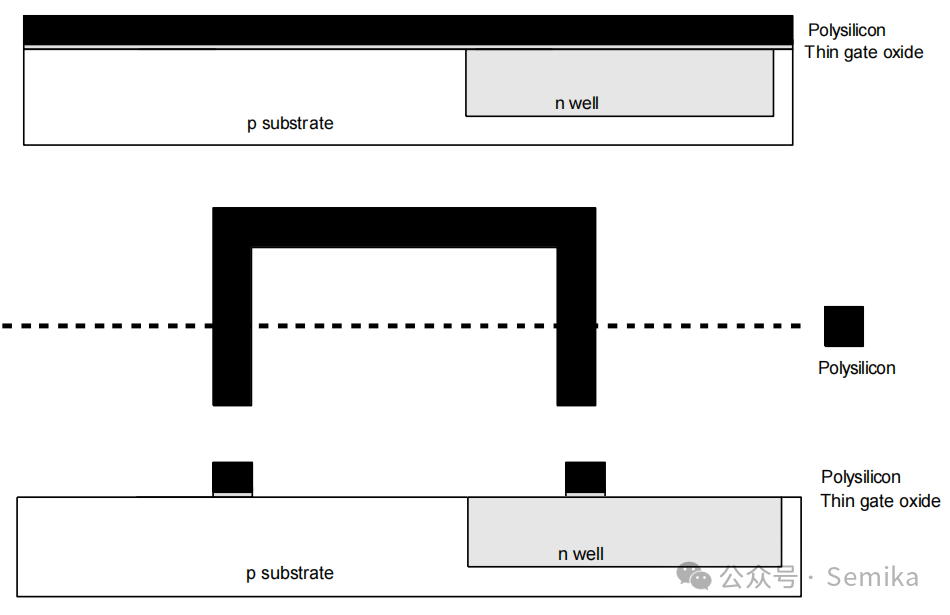
Semiconductor Manufacturing Process – Photolithography
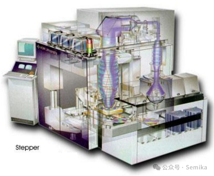
The photolithography machines frequently mentioned in recent years are just one of many process equipment. Even in lithography, there are many processes and devices involved.
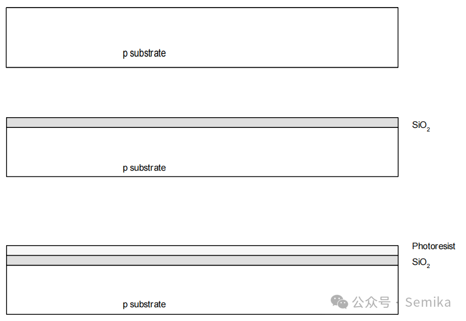
(1) Photoresist Coating
Photoresist is a light-sensitive material. A small amount of photoresist liquid is applied to the wafer. The wafer spins at speeds from 1000 to 5000 RPM, spreading the photoresist into a uniform layer 2 to 200um thick.
There are two types of photoresist: negative and positive.
Positive resist: Exposed to light can decompose complex molecular structures, making them easier to dissolve.
Negative resist: Exposure makes the molecular structure more complex and harder to dissolve.
The steps involved in each lithography step are as follows:
◈ Clean the wafer
◈ Deposit barrier layers SiO2, Si3N4, metals
◈ Apply photoresist
◈ Soft bake
◈ Align mask
◈ Expose pattern
◈ Develop
◈ Bake
◈ Etch
◈ Remove photoresist
(2) Pattern Preparation
IC designers use CAD software to design the pattern for each layer. The pattern is then transferred to an optically transparent quartz substrate (template) using a laser pattern generator or electron beam.
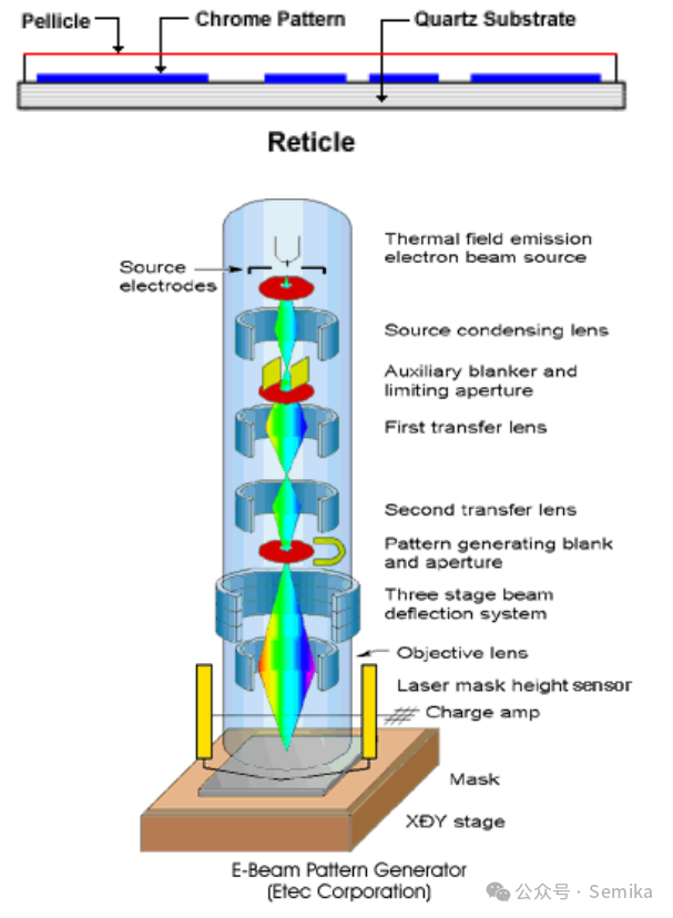
(3) Pattern Transfer (Exposure)
Here, a photolithography machine is used to project the pattern from the template onto the chip layer.
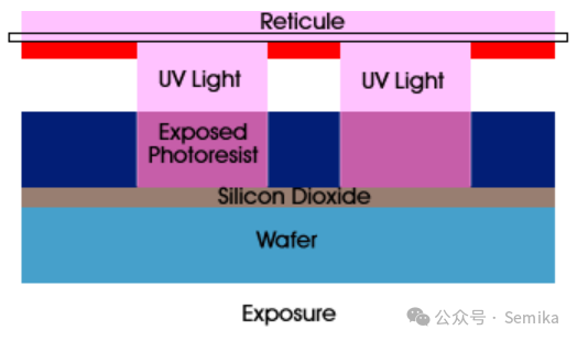
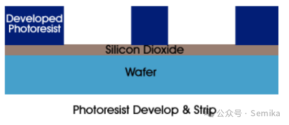
(4) Development and Baking
◈ After exposure, the wafer is developed in an acid or alkaline solution to remove the exposed areas of photoresist.
◈ Once the exposed photoresist is removed, the wafer is “baked” at low temperatures to harden the remaining photoresist.
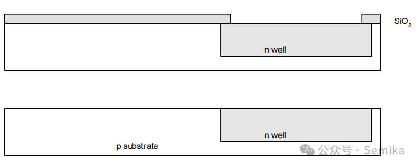
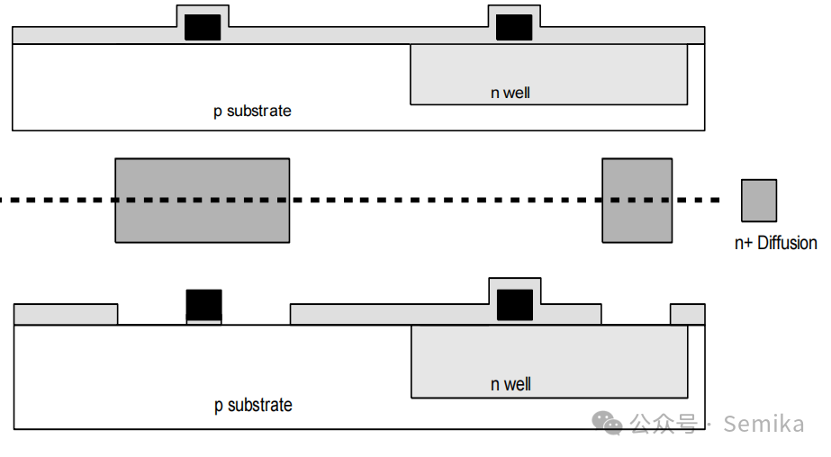
Semiconductor Manufacturing Process – Etching and Ion Implantation
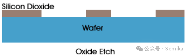
(1) Wet and Dry Etching
◈ Chemical etching is performed on large wet platforms.
◈ Different types of acids, bases, and caustic solutions are used to remove selected areas of different materials.
◈ BOE, or buffered oxide etchant, is prepared with ammonium fluoride buffered hydrofluoric acid, used to remove silicon dioxide without etching the underlying silicon or polysilicon layers.
◈ Phosphoric acid is used to etch silicon nitride layers.
◈ Nitric acid is used to etch metals.
◈ Sulfuric acid is used to remove photoresist.
◈ For dry etching, the wafer is placed in an etching chamber and etched through plasma.
◈ Personnel safety is a top priority.
◈ Many wafer fabs use automated equipment to perform the etching process.
(2) Photoresist Stripping
Then the photoresist is completely stripped from the wafer, leaving an oxide pattern on the wafer.
(3) Ion Implantation
◈ Ion implantation alters the electrical properties of specific areas within existing layers on the wafer.
◈ Ion implanters use high-current accelerator tubes and steering focus magnets to bombard the wafer surface with ions of specific dopants.
◈ As the dopant chemicals deposit on the surface and diffuse into it, the oxide acts as a barrier.
◈ The silicon surface is heated to 900℃ for annealing, allowing the implanted dopant ions to further diffuse into the silicon.
Semiconductor Manufacturing Process – Thin Film Deposition
There are many methods and contents for thin film deposition, detailed below:
(1) Silicon Dioxide
When silicon is present in oxygen, SiO2 grows thermally. The oxygen comes from either oxygen or water vapor. The required environmental temperature is 900 ~ 1200℃. The chemical reactions that occur are
Si + O2 → SiO2
Si + 2H2O → SiO2 + 2H2
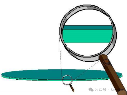
The surface of the silicon wafer after selective oxidation is shown below:
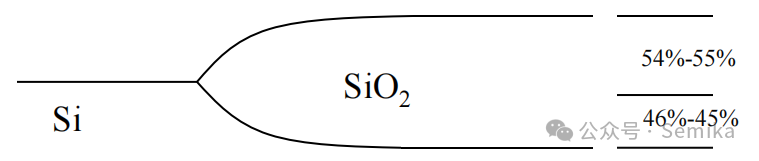
Oxygen and water will diffuse through the existing SiO2 and combine with Si to form additional SiO2. Water (vapor) diffuses much more easily than oxygen, so the growth rate of vapor is much faster.
Oxides are used to provide insulation and passivation layers, forming transistor gates. Dry oxygen is used to form gates and thin oxide layers. Vapor is used to form thick oxide layers. The insulating oxide layer is usually around 1500nm, while gate layers typically range from 200nm to 500nm.
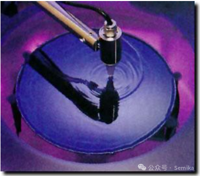
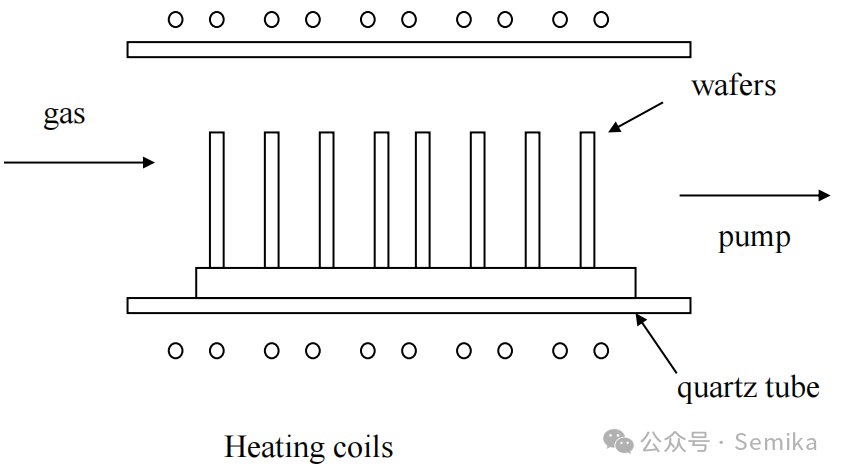
(2) Chemical Vapor Deposition
Chemical vapor deposition (CVD) forms thin films on the substrate surface through thermal decomposition and/or reactions of gaseous compounds.
There are three basic types of CVD reactors:
◈ Atmospheric Chemical Vapor Deposition
◈ Low Pressure CVD (LPCVD)
◈ Plasma Enhanced CVD (PECVD)
The schematic diagram of the low-pressure CVD process is shown below.
The main CVD reaction processes are as follows:
i). Polysilicon
SiH4 → Si + 2H2 (600℃)
Deposition rate 100 – 200 nm/min
Doping gases such as phosphorus (phosphine), boron (diborane), or arsenic can be added. Polysilicon can also be doped using diffusion gases after deposition.
ii). Silicon Dioxide
SiH4 + O2 → SiO2 + 2H2 (300 – 500℃)
SiO2 serves as an insulator or passivation layer. Phosphorus is often added to improve electronic flow performance.
iii). Silicon Nitride
3SiH4 + 4NH3 → Si3N4 + 12H2
(Silane) (Ammonia) (Nitride)
(3) Sputtering
The target is bombarded by high-energy ions such as Ar+, causing atoms in the target to be displaced and transported to the substrate.
Metals such as aluminum and titanium can be used as targets.
(4) Evaporation
Al or Au (gold) is heated to its evaporation point, and the vapor condenses to form a thin film covering the surface of the wafer.
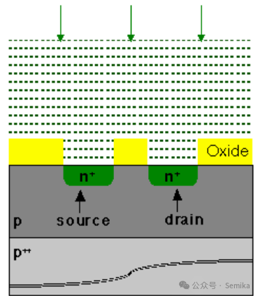
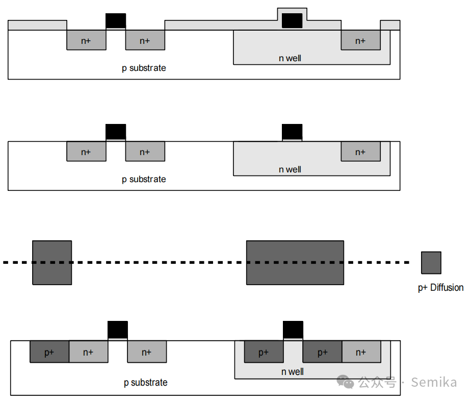
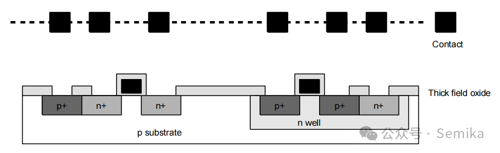
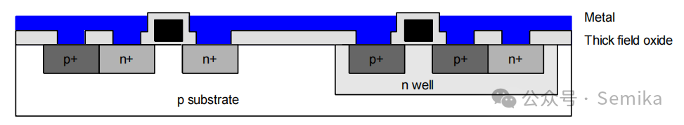
The following is a case study to detail how the circuit on the wafer is formed step-by-step through lithography, etching, and ion deposition:
Semiconductor Manufacturing Process – Packaging and Testing
(1)Probe Test
After the final circuit preparation is completed, automated probe testing methods are used to test the devices on the wafer, eliminating defective products.
(2)Wafer Dicing
After probe testing, the wafer is cut into individual chips.
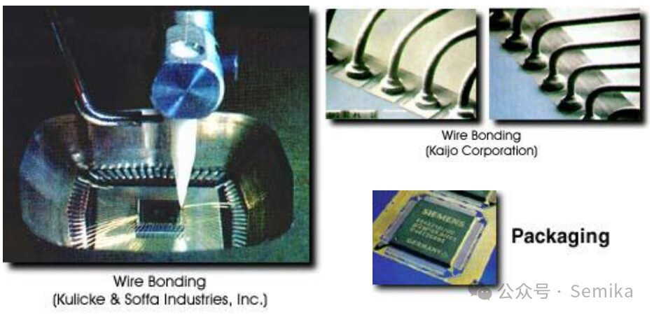
(3) Wire Bonding and Packaging
◈ Individual chips are connected to a lead frame, with aluminum or gold wires connected through thermal compression or ultrasonic welding.
◈ Packaging is completed by sealing the device in ceramic or plastic packaging.
◈ Most chips also require final functional testing before being delivered to downstream users.
END
The reproduced content only represents the author’s views
It does not represent the position of the Semiconductor Research Institute of the Chinese Academy of Sciences
Editor: Schrödinger’s Cat
Responsible Editor: Muxin
Submission Email: [email protected]