Click on “Two Monkeys Club“
Follow Us
Table of Contents
-
00 Project Overview
-
01 Synchronization Processing of Asynchronous Clocks
-
02 FIFO Design (Part 1)
-
03 FIFO Design (Part 2)
-
04 Baud Rate Design
-
05 Data Reception Section
-
06 Data Transmission Section
-
07 Simulation Framework
-
08 Baud Rate Model and Register Operations
-
09 Data Transmission Model
-
10 Data Reception Model
-
11 Data Comparison and Interrupt Check
-
12 Testcase
-
13 Common Interview Questions Related to the Project
Functionality
Implement a UART module (Universal Asynchronous Receiver/Transmitter) connected via the APB bus in ARM, including both design and verification parts.
Project Requirements
-
The maximum operating frequency of the system clock is 100MHz, and the functional clock is 26MHz.
-
Reset functionality for both system and functional clock domains.
-
The configuration interface meets the AMBA2.0-APB bus interface timing, with a bus width of 16 bits.
-
Data transmission meets general serial port timing, with configurable parity functionality.
-
Baud rate meets 115200, or is configurable.
-
Receive and transmit FIFO reset can be controlled separately, with configurable trigger depth.
-
Data transmission and reception interrupt functionality is configurable.
-
Data transmission interval is controllable.
-
Includes status indication functionality.
-
Includes FIFO data quantity indication functionality.
Framework
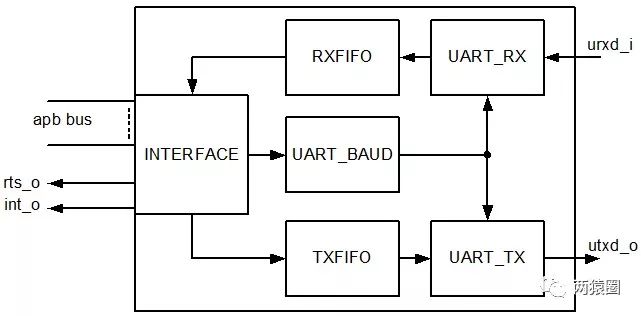
Design
-
Baud Rate Generation Module
-
Generates the receive and transmit baud rate clock based on the functional clock and configuration.
-
Data Reception
-
Receives data based on the RX baud rate clock, performs parity check, stores data in the RX FIFO, and is read by the CPU via the APB bus. Contains a receive data state machine.
-
Data Transmission
-
The CPU places the data to be sent into the TX FIFO via the APB bus, and transmits data based on the TX baud rate clock. Contains a transmit data state machine.
-
Register Configuration
-
Implements APB read/write register functionality, interrupt operations, function selection, module status indication, etc.
Verification
-
Baud Rate Generation
-
Generates the baud rate clock used in the simulation environment.
-
Data Reception
-
Data reception model in the simulation environment.
-
Data Transmission
-
Data transmission model in the simulation environment.
-
APB Bus
-
APB bus model in the simulation environment, simulating CPU response to interrupts and implementing various functions.
-
Data Comparison
-
Generates different comparison results based on the comparison of transmitted and received data and timing, facilitating observation of results during simulation.
-
Testcase Generation
-
Generates different cases through various stimuli or configurations to verify if the functionality meets requirements.
AMBA-APB Protocol
AMBA The AMBA bus is an advanced microcontroller bus architecture developed by ARM, defining a standard for on-chip communication when designing high-performance embedded microcontrollers. AMBA2.0 defines three different buses: AHB, ASB, and APB.
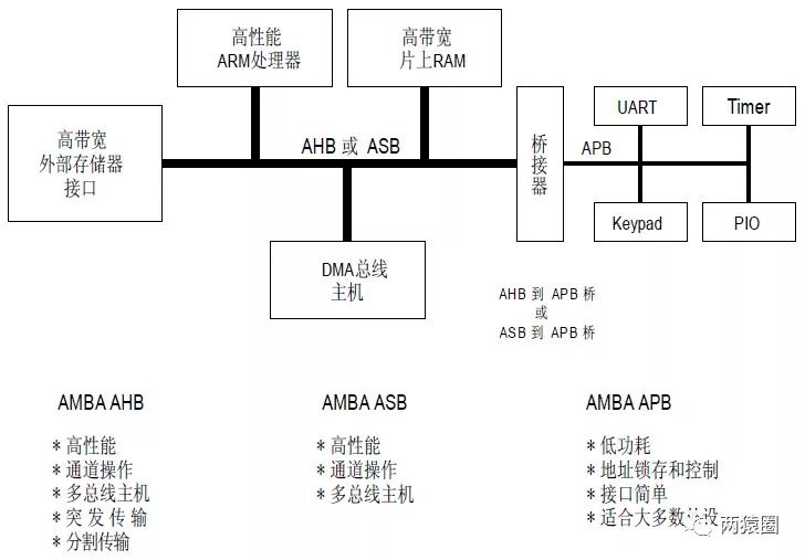
A typical AMBA-based microcontroller consists of a high-performance central bus (AHB or ASB) that supports high-bandwidth external memory, including CPU, on-chip memory, and other direct memory access (DMA) devices. This bus provides a high-bandwidth interface for most transfers between the aforementioned units. There is also a bridge on this high-performance bus to connect to the lower bandwidth APB, which connects most of the system peripherals.
APB
-
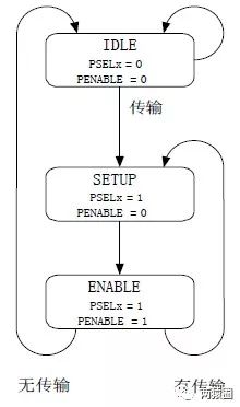
Interface Signals
PCLK (input): The clock for the APB bus, all transfers are synchronized to its rising edge. PRESETn (input): The reset signal for the APB bus, active low. PADDR (input): The address bus for the APB. PSELx (input): The selection signal for the APB module, active high. This signal selects the module that needs to transfer data over the APB bus. PENABLE (input): The trigger signal for the APB module, indicating the second clock cycle of the APB transfer. PWRITE (input): Write (active high) and read (active low) signal on the APB bus. PWDATA (input): The write data signal on the APB bus, driven by the APB bus bridge. PRDATA (output): The read data signal on the APB bus, driven by the APB module. Notes:
APB bus transfers require two clock cycles.
Input and output are relative to the APB module (slave).
A “write” operation transfers data from the APB bus to the APB module, while a “read” operation transfers data from the APB module to the APB bus.
-
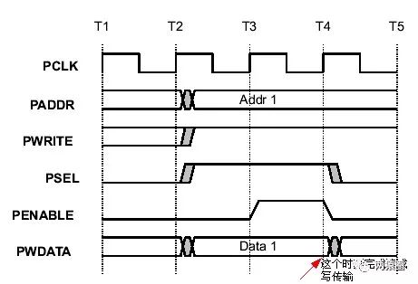
APB Write Operation
-
The PADDR, PWRITE, PSEL, and PWDATA signals are valid at the same time. If there is only one “write” operation, the above signals last for two cycles. If there are multiple “write” operations (e.g., in Burst mode), PWRITE and PSEL can remain unchanged, while PADDR and PWDATA change every two cycles.
-
The PENABLE signal is valid one cycle after PSEL is valid and lasts for one cycle. If there are multiple “write” operations, the PENABLE signal remains low for one cycle and high for one cycle within every two cycles.
-
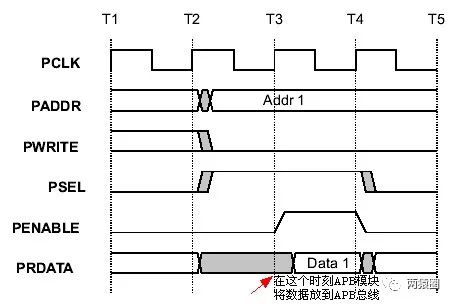
APB Read Operation
-
The PADDR, PWRITE, and PSEL signals are valid at the same time. If there is only one “read” operation, the above signals last for two cycles. If there are multiple “read” operations (e.g., in Burst mode), PWRITE and PSEL can remain unchanged, while PADDR changes every two cycles.
-
The PENABLE signal is valid one cycle after PSEL is valid and lasts for one cycle. If there are multiple “read” operations, the PENABLE signal remains low for one cycle and high for one cycle within every two cycles.
- The APB module needs to send the required data for the “read” operation to the APB bus during the valid PENABLE period and maintain it for one cycle.
Long
Press
Close
Note
Two Monkeys Club
WeChat ID: twomonkeysclub
Programmers who understand a bit about the internet and IC.
Helping you enrich your project experience and easily navigate campus recruitment.

I know you are watching!