Regarding the idea of layered design, a detailed design process was explained in a previous article titled “Embedded Hardware Communication Interface Protocol-SPI (Part 2) Layered Architecture Design Simulation Interface” when discussing SPI interface design, so I won’t elaborate further here.
Now, using the BSP layer design approach of SPI as a reference, we will use the same method to design the BSP layer code module for the IIC interface.
The content to be explained and implemented in this article is mainly divided into two parts: code implementation of IIC interface management and code implementation of IIC timing.
-
IIC Interface Management
The purpose of interface management is to allow multiple IIC interfaces to be used in one project during future expansions.
For now, we will not consider using complex data structures, but will simply use basic macro definitions placed in header files to avoid troublesome memory allocation and management operations.
Starting with IIC interface number “1”, when adding new IIC interfaces, simply refer to the current example to define subsequent IIC interface numbers and pins:
#define IIC_1 1
#define IIC1_PORT_SCL PORTB
#define IIC1_PIN_SCL 6
#define IIC1_PORT_SDA PORTA
#define IIC1_PIN_SDA 2
The implementation here is still in the BSP layer’s IIC module code, which sits between chip drivers (registers) and application libraries. It must consider future portability and development, as this IIC module may be implemented by IO simulation or by demo drivers provided by the chip manufacturer, so the encapsulated BSP layer interface must consider future expansion.
Thus, the approach is to pass all parameters through functions, and design them to return a value of type uint8_t. This design choice is based on habit and can be referenced in the article titled “【Embedded Programming】Function Return Type Design“.
By opening the STM32CubeMX tool, we can see that when configuring the IIC interface, the configurable parameters are as shown in the screenshot below:
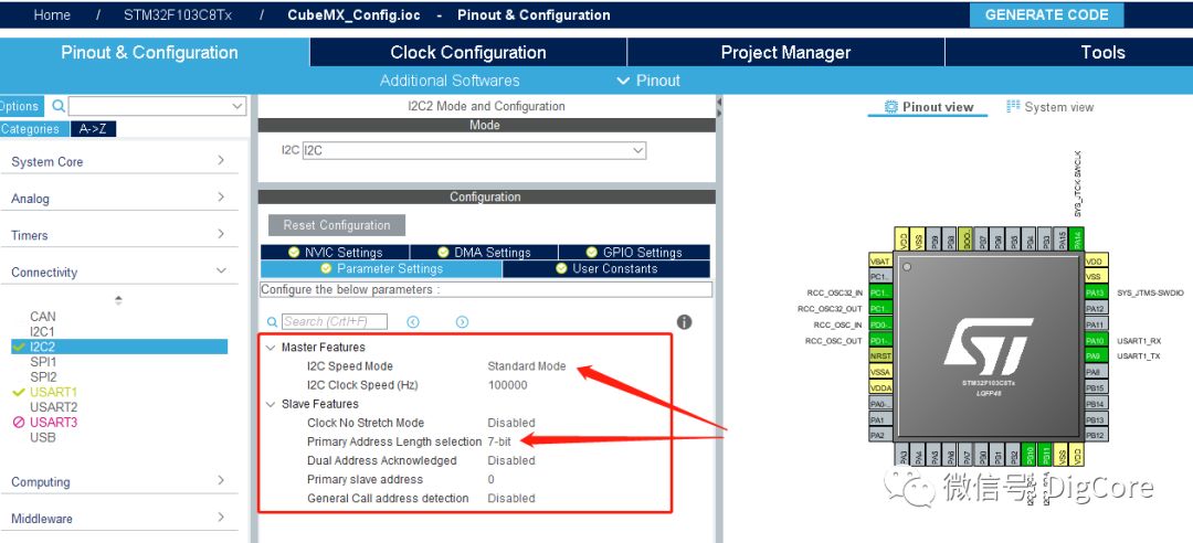
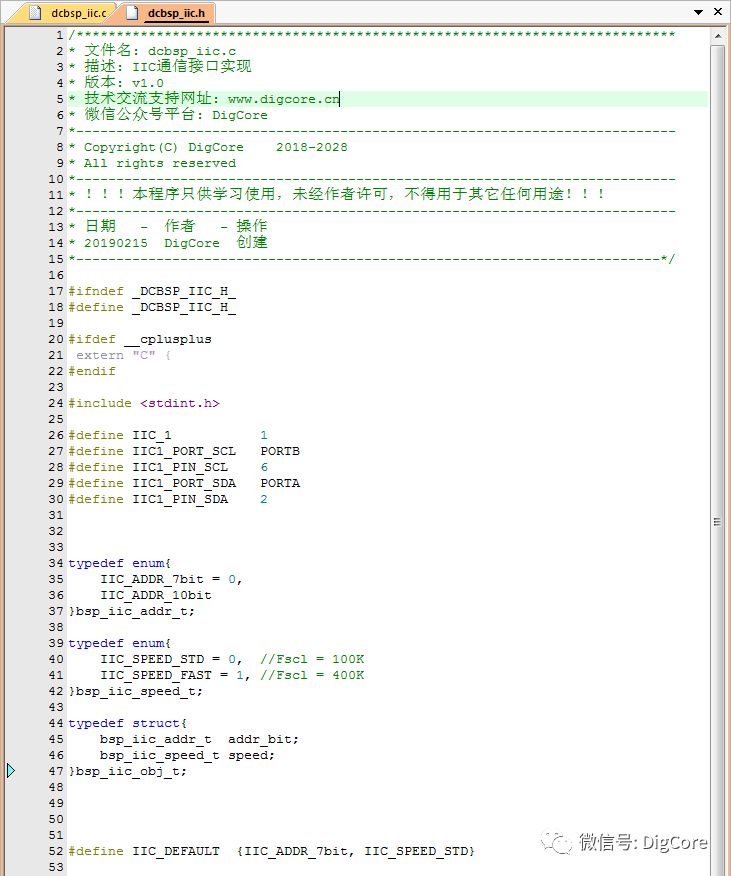
Based on the above, we will define an IIC interface object in the structure, including address width and clock rate, as shown in the bsp_iic_obj_t structure type in the header file.
-
IIC Timing
From the previous article “Embedded Hardware Communication Interface Protocol – IIC (Part 1) Protocol Basics”, we know that there are several signal characteristics in the timing of IIC. Now we will implement them one by one using code.

In fact, there are already many implementations of IIC timing simulation on the internet. The simplest can be found in the open-source community on GitHub, Baidu Encyclopedia, and various technical websites, with many technical forums hosting IIC application examples and source code.
Therefore, the simulation of IIC timing has become quite standardized. However, the purpose of “reinventing the wheel” here is to integrate, optimize, and improve the BSP layer code of our own project, enhancing the project’s extensibility and application, which greatly benefits the overall framework of the code!
In short, I want to write this article in detail. Without further ado, let’s get to the code:
-
Start Flag:
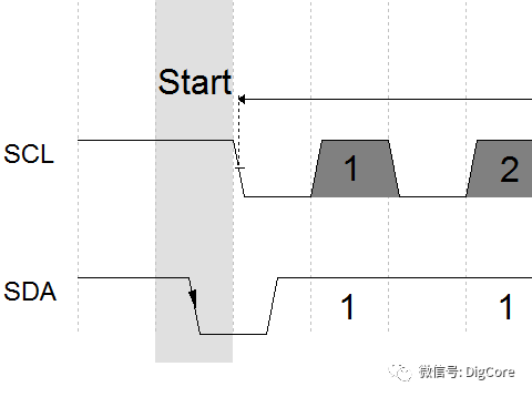
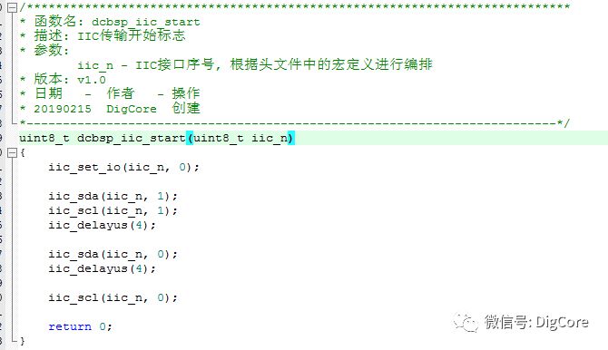
The code for this start flag is quite simple. First, ensure that the SDA pin being used is set to output. In this BSP layer’s IIC module, the iic_set_io(iic_n, 0); function is used to set the SDA pin of the specified IIC interface number as output. The subsequent level settings complete the signal timing process.
-
End Flag
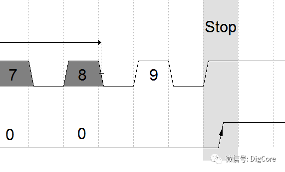
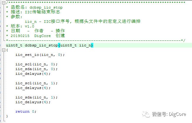
The approach is similar to the previous one, so I’ll skip the details.
-
Data Output
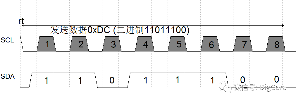
The above example sends a hexadecimal data 0xDC with a timing diagram. The most important principle is that: SCL must be low before changing the SDA output data; when SCL is high, the SDA must remain stable and unchanged.
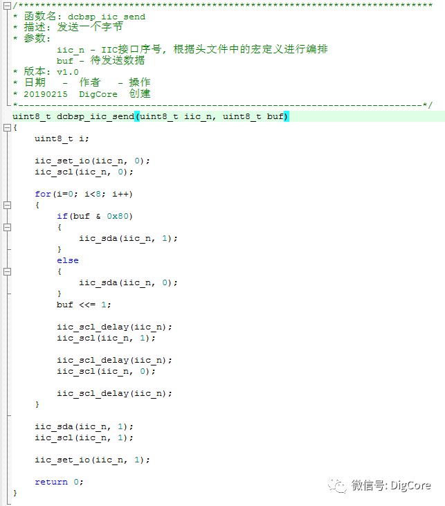
The process of implementing the code is similar to the SPI simulation, where data bits are output one by one, shifting the data with each bit output, as in “buf <<= 1;” so that the next bit is output when SCL goes low again.
After completing the output, immediately set the SDA IO pin to input mode by calling iic_set_io(iic_n, 1); function.
-
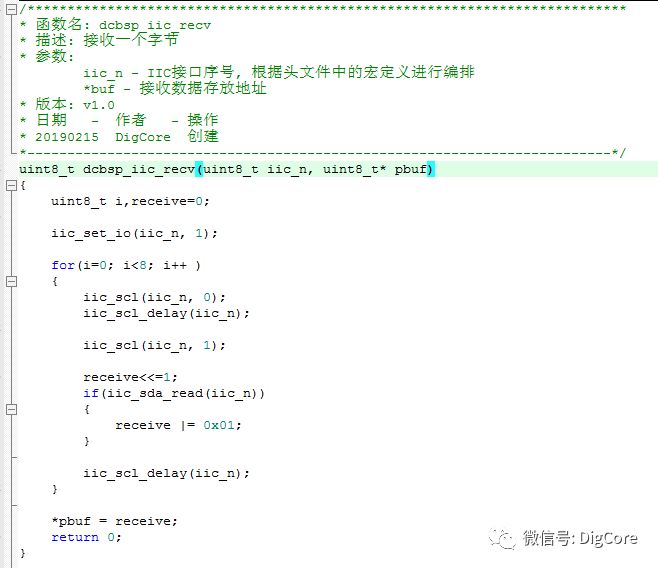
Data Sampling
Similar to data transmission, bits are sampled on the rising edge of SCL. Here, data sampling refers to the IIC master receiving data sent from peripheral devices. The most important principle is: SCL must be low for a delay to ensure that the SDA data is stable; when SCL is high, read the SDA pin level.
-
ACK/NACK Acknowledgement
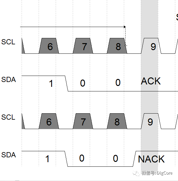
From the timing diagram, we can see that the difference between the ACK and NACK response bits lies in the level state of SDA during the high period of the 9th SCL.
From the previous article, we know that the IIC bus circuit connections generally have pull-up resistors Rp for both SCL and SDA. This means that if the IIC slave device does not generate a signal due to absence (hardware not soldered), malfunction (burnt out), or other reasons, the SDA will be in a NACK state, which means that the IO pin level is pulled high by the pull-up resistor, which can be understood as a “default” level without a “response”.
The purpose of the acknowledgment is to inform the “sender” that the “receiver” has successfully received the data that was just sent.
-
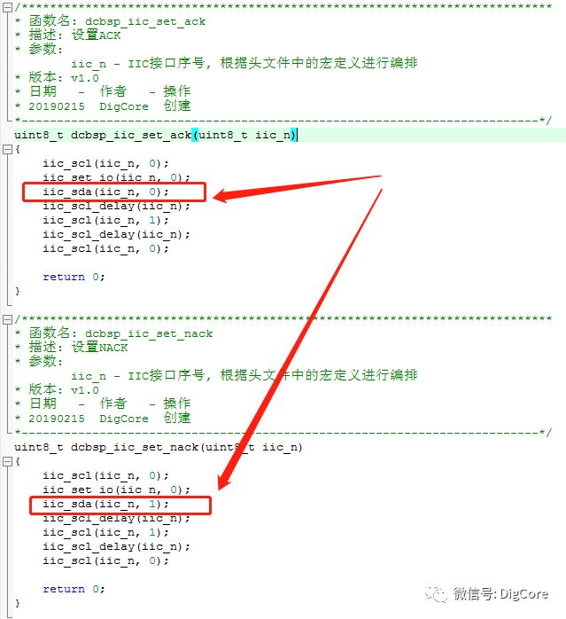
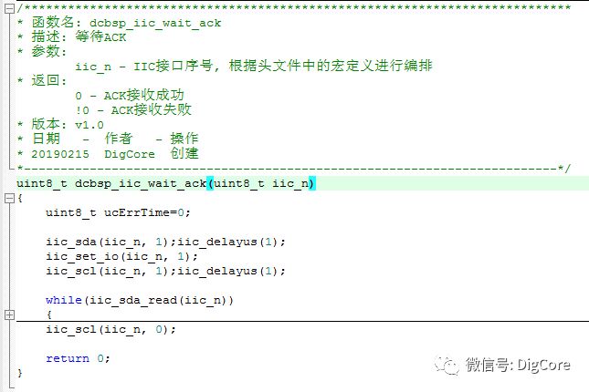
Wait for ACK Response
Since it is an acknowledgment, there is a bidirectional nature: the IIC slave acknowledges the IIC master; the IIC master acknowledges the IIC slave.
The ACK/NACK response shown in the above diagram is actively output by the IIC master to inform the slave, “I have received the data normally.”
Meanwhile, the IIC slave informs the master with an ACK response, which requires the concept of waiting for ACK. The master detects the ACK signal by reading the SDA pin level.
The above timing is simulated using GPIO pins, encapsulated into the DigCore_Embed embedded software architecture’s BSP layer interface, providing the IIC hardware interface to the upper layer while simulating GPIO and timing operations. During the porting process, adjustments can be made within these encapsulated interfaces based on the target platform.
For instance, replacing the GPIO simulation scheme with the official demo program only requires modifying the code in the above interfaces, and the upper application libraries, whether for the temperature and humidity sensor SHT20, EEPROM storage chip AT24C1024B, or the BS81163-A touch keyboard chip, which all use the BSP layer’s IIC interface, do not need any modifications.
This is the advantage of the layered design philosophy in embedded software.
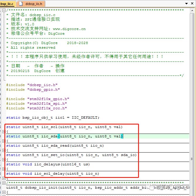
The interfaces called internally by the above functions are all static functions in the current BSP layer’s IIC module source code:
In summary, the simulation of IIC timing is mainly based on the characteristics of IIC timing, creating corresponding delays after each signal to achieve the timing presentation! The challenge lies in breaking down the IIC timing into multiple signal characteristics for simulation. If one doesn’t have a deep understanding of the signal timing diagram, it can be quite confusing when comparing it with the code, requiring careful verification!
The above code only completes the initial writing and organization and has not been validated on specific peripherals. The final source code for this BSP layer’s IIC module will be shared in the next installment!
★★★★★ Recommended Articles
“【Embedded Programming】Function Return Type Design”
“【Embedded Programming】Solutions for Endianness Storage Differences”
“Embedded Hardware Communication Interface – Using RingBuffer for Data Processing (Part 2) Detailed Design Process”
“Embedded Hardware Communication Interface – Using RingBuffer for Data Processing (Part 1)”
“Rapid Development of MQTT (Part 1) MQTT from the Perspective of Electronic Engineers”
“Rapid Development of MQTT (Part 2) Introduction to MQTT”
“Building an MQTT Client – The Clearest MQTT Protocol Architecture”
“Setting Up an MQTT Server – The Fastest Way to Validate Your Developed Client”
★★★★★ Similar Articles
“Embedded Hardware Communication Interface Protocol – UART (Part 5) Packet Design and Parsing”
“Embedded Hardware Communication Interface Protocol – UART (Part 4) Application Layer Protocol Design”
“Embedded Hardware Communication Interface Protocol – UART (Part 3) Quick Use of Serial Port and Applications”
“Embedded Hardware Communication Interface Protocol – UART (Part 2) Standards Under Different Electrical Specifications”
“Embedded Hardware Communication Interface Protocol – UART (Part 1) Protocol Basics”
“Embedded Hardware Communication Interface Protocol – SPI (Part 3) Simulation Interface Applications”
“Embedded Hardware Communication Interface Protocol – SPI (Part 2) Layered Architecture Design Simulation Interface”
“Embedded Hardware Communication Interface Protocol – SPI (Part 1) Protocol Basics”
“Embedded Hardware Communication Interface Protocol – IIC (Part 1) Protocol Basics”
★★★★★ Further Reading
“【Hardware Circuit】Altium Designer 18 Rule Check Meanings”
“【Hardware Circuit】Basic Principles and Application Cases of N-Channel and P-Channel MOSFETs”

www.digcore.cn
More technical content awaits you!
Long press the QR code to follow us