Click to follow Asynchronous Books, pin the public account
Sharing IT good books, technical dry goods, and workplace knowledge with you every day
Participate in the topic discussion at the end of the article, and receive Asynchronous Books daily.
—— Asynchronous Editor
The Eternal Hotspot — CPU
Lights, waiting for the lights…
—— Intel
If we were to select the classic tech advertisement music from the past decade, Intel’s advertisement music “Lights, waiting for the lights…” would surely be on the list. The familiar blue label “Intel Inside” is also a highly recognizable advertisement icon.
The Central Processing Unit (CPU), though well-known to the public, has long been synonymous with high-end and sophistication. Do you share the same impression? In early computer magazines, there were always extensive sections and columns detailing the specifications of CPU chips released by Intel or AMD, as well as the advantages and disadvantages of MIPS and ARM, and even the intriguing rumors and behind-the-scenes stories of various CPUs.
Moreover, the high-end technology represented by CPUs has always been shrouded in a veil of mystery. The CPU design department always attracts numerous candidates competing for positions. It is not an exaggeration to say that just as every boy has a dream of being a soldier, it seems that every chip designer has a CPU dream.
Today, I will introduce two books: “Hand-in-Hand Guide to CPU Design” and “Homemade Programming Language”, and bring forth some thoughts from the author Hu Zhenbo on self-made CPUs. I hope to provide some guidance for readers interested in this field.
(Published in May 2018)
(Published in May 2018)
History
Chips are the cornerstone of the entire electronic information industry. Currently, the global semiconductor market size reaches $320 billion, with 54% of chips exported to China, yet the market share of domestic chips only accounts for 10%. The Chinese chip industry consumes over $200 billion in foreign exchange for imports annually, surpassing oil and bulk commodities, and occupies a significant proportion of imported goods.
The CPU, as the “heart” of chips, can be said to be the “heart of hearts.” The domestic industrial strength in this area has always been relatively weak. The realization of domestic autonomy for CPUs is crucial for our development, but the mainstream instruction set architectures (such as x86 and ARM) have always been monopolized by foreign companies, forcing domestic companies to pay exorbitant patent fees and be constrained. As a special type of chip, the CPU requires the instruction set architecture to have universal applicability and the ability to share ecosystems, so inventing a closed instruction set within a single country is impractical; it must align with the world’s mainstream architectures. Against this backdrop, the open RISC-V architecture brings tremendous strategic opportunities for the development of China’s CPU chip industry, hoping to achieve complete domestic autonomy and mainstream architecture for CPUs.
Currently, our country is at a critical period of vigorously developing the chip design industry; the great rejuvenation of the Chinese nation requires extensive scientific research and engineering workers to work tirelessly and strive, and many pragmatic technical backbones like the author to shoulder the responsibility of revitalizing domestic chips. The long-standing shortage of talent in the domestic CPU field is a major factor restricting the industry’s development. The author of “Hand-in-Hand Guide to CPU Design”, as a senior CPU design expert working on the front lines for many years, has compiled his experience into a book, with detailed information and lively writing. Coupled with the example of the E200 series processor core developed by the author’s company, it is very suitable for teaching and enthusiasts’ learning, and has a very positive significance for popularizing CPU design technology.
The emerging RISC-V architecture has already sparked a global trend and has received widespread attention domestically. However, due to the lack of good Chinese popularization books, many people are still “hearing its name but not seeing its form” regarding RISC-V. The author, as one of the first technical experts in the country to contact the RISC-V architecture and successfully develop RISC-V processors, has open-sourced the processor cores he developed in his spare time and published a book detailing its implementation details, reflecting his high professional level and strong feelings for promoting the development of domestic CPU industry.
ISA Must Bear This Burden — Why Domestic CPUs Have Not Yet Succeeded Sufficiently
It is well known that chips are the core area of China’s information industry development, and CPUs represent the core technology in chips. In this regard, there is a significant gap between our country and developed countries . Although after years of effort, the technological gap has been significantly narrowed, there are still not many domestic CPUs in the civil commercial field. What causes the current situation where domestic commercial CPUs have not yet succeeded sufficiently? Next, we will list the companies developing CPUs independently in China and their current situation, as well as the instruction set factions they have chosen. By analyzing their past and present one by one, we believe that readers will find answers.
The emerging RISC-V architecture has already sparked a global trend and has received widespread attention domestically. However, due to the lack of good Chinese popularization books, many people are still “hearing its name but not seeing its form” regarding RISC-V. The author, as one of the first technical experts in the country to contact the RISC-V architecture and successfully develop RISC-V processors, has open-sourced the processor cores he developed in his spare time and published a book detailing its implementation details, reflecting his high professional level and strong feelings for promoting the development of domestic CPU industry.
1. Loongson
The Loongson CPU is developed by the Loongson Project Group of the Institute of Computing Technology, Chinese Academy of Sciences, and is researched and developed by Beijing Shenzhou Longxin Integrated Circuit Design Company authorized by the Institute of Computing Technology, Chinese Academy of Sciences. Here is a brief introduction to the Loongson CPU chip.
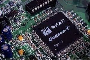
· The frequency of Loongson 1 is 266MHz, first used in 2002, as shown in Figure 1-3.
· The maximum frequency of Loongson 2 is 1GHz.
· The Loongson 3A series is a domestic commercial quad-core processor. The latest Loongson 3A3000 is based on the 28nm FDSOI process, designed as a 4-core 64-bit processor, with a main frequency of 1.5GHz and a power consumption of only 30W, making it very suitable for notebook platforms.
· The Loongson 3B series is a domestic commercial octa-core processor, with a main frequency exceeding 1GHz, supporting vector computation acceleration, and a peak computing capability of 128GFLOPS, boasting a high performance-to-power ratio. The Loongson 3B series is mainly used in high-performance computers, high-performance servers, digital signal processing, and other fields.

2. Junzheng
Another company in the domestic MIPS camp is Beijing Junzheng. Junzheng and Loongson belong to the MIPS camp; unlike Loongson’s focus on desktop PC processors, Beijing Junzheng is one of the earliest local IC design companies focused on wearables and the Internet of Things. Since embedded chip software is generally customized according to demand, many wearable products and applications in the smart wearable market have special features, leading to a relatively short software ecosystem due to the diversity of application needs, making it impossible for a single vendor to achieve monopoly. Therefore, it is not easy for the smart wearable market to see the same situation as the x86 and ARM architectures dominating the PC and mobile phone markets.
Smart wearable chips and IoT chips do not have high performance requirements; most application scenarios pay more attention to low power consumption, low cost, and size. Junzheng’s products fully meet performance requirements; x86 processors cannot be applied in this field, while ARM camp IC design companies are constrained by relatively high licensing fees, which do not provide price competitiveness when chip production is low. Junzheng has over a decade of chip design experience and technical accumulation, and its greatest feature is its high performance-to-power ratio. The first batch of domestically listed smartwatches, including the first-generation smartwatch from Guoke, Tuman Generation 1, and Tuman Generation 2 smartwatches, all adopted Junzheng’s solutions.
1. Beijing University of Posts and Telecommunications
Beijing University of Posts and Telecommunications Micro System Technology Co., Ltd. was established in November 2002 and is an important backbone enterprise in the national integrated circuit design industry. In 2005, AMD reached an agreement with the Chinese government, and the Ministry of Science and Technology designated the Microelectronics Center of Peking University to receive the technical authorization of the AMD Geode-2 processor, which undoubtedly belongs to the x86 architecture, thus China obtained x86 technology. However, the Geode processor belongs to AMD’s embedded processors, so the x86 technology authorized to Peking University belongs to the embedded architecture.
2. Zhaoxin
Another domestic company using the x86 architecture that may be more familiar to many is Zhaoxin. It is well known that the core x86 architecture is the core technology of Intel and AMD, and the U.S. government strictly controls the authorization of its technology. However, besides Intel and AMD, another Taiwanese company, VIA, also once had the authorization for the x86 architecture. It is reported that, as shown in Figure 1-8, Zhaoxin’s self-developed ZX-C processor went into mass production in April 2015, using a 28nm process, a quad-core processor with a frequency of up to 2.0GHz, and supports national secret algorithm encryption. In 2017, Zhaoxin announced that its latest generation ZX-D series quad-core and octa-core general-purpose processors had successfully taped out and revealed that a 16nm ZX-E octa-core CPU would be launched in 2018.
3. Haiguang
In addition to Shanghai Zhaoxin, there is a newly established company — Tianjin Haiguang. In 2016, AMD announced an agreement with Tianjin Haiguang Investment Company, authorizing x86 technology to Haiguang, receiving authorization fees, and both parties would also establish a joint venture to authorize the production of server processors. It is said that to enter the high-performance server market in China, the x86 technology authorized to Chinese companies by AMD is likely to be the most advanced x86 technology. We look forward to Haiguang’s performance.
The blue giant IBM’s Power architecture has always been a representative of high performance. In 2013, IBM established the OpenPower alliance in conjunction with NVIDIA and other companies, allowing other companies to obtain Power architecture authorization. It then promoted the establishment of the China POWER Technology Industry Ecological Alliance, signing authorization agreements with several Chinese companies, including Zhongsheng Hongxin. Zhongsheng Hongxin was established in 2013, and it is believed that Hongxin will achieve technological digestion and absorption and innovation in several years.
Shenwei processors or Shenwei CPUs, abbreviated as “SW processors”.
Shenwei continues to deepen and upgrade its self-developed Alpha architecture, expanding multi-core architectures and SIMD and other special extended instruction sets, mainly targeting high-performance computing and server fields. In 2016, at the International Supercomputing Conference, the “Sunway TaihuLight” supercomputer system based on the Shenwei 26010 processor (as shown in Figure 1-9) made its debut and won the championship, achieving a peak performance of 12.5×10^18 floating-point operations per second, becoming the world’s first supercomputer with a running speed exceeding 10^18 operations per second.
To better understand the content of this section, it is necessary to introduce the authorization model of ARM. In short, ARM’s main authorization models can be divided into two types.
· Authorizing “ARM Processor IP” to other chip manufacturers (partners), who directly use ARM Processor IP to design SoC chips.
· Authorizing “ARM Architecture” to other chip manufacturers (partners), who self-develop their processor cores based on ARM architecture, and then use their self-developed processor cores to design SoC chips.
1. Feiteng
Feiteng Company is one of the most powerful chip developers in China, established by the high-performance processor research team of the National University of Defense Technology. For many years, the National University of Defense Technology has accumulated strong technical strength in the CPU field. In 2016, Tianjin Feiteng announced its latest product FT2000, which first appeared at the 2015 HotChips conference, codenamed “Mars”, targeting high-performance servers and industry business hosts. FT2000 adopts the ARMv8 instruction set but uses self-developed cores, different from the Cortex-A53/A57/A72 cores directly purchased from ARM.
FT2000 is noteworthy for its performance, featuring up to 64 FTC661 processor cores, with reported scores of 672 for integer and 585 for floating-point in the Spec 2006 test, comparable to the Xeon E5-2699v3. This also marks the first time a domestic server chip has matched Intel in performance; the total aggregated bandwidth of the memory controller chip is 204.8GB/s, exceeding the current E5V3 and E7V3, and approaching IBM POWER8 (230GB/s). Scoring comparable to Intel’s Xeon E5-2699v3 indicates that Feiteng 2000 is already sufficient for many commercial applications; as long as the software ecosystem keeps up, it can fully replace certain Intel products in the commercial market.
2. Huawei HiSilicon
Huawei HiSilicon is currently one of the most powerful chip developers in China. Huawei’s Kirin chips are on par with leading chip companies like Qualcomm and Samsung in performance. At the same time, Huawei is also one of the four major server providers in China, with Huawei, Lenovo, Inspur, and other domestic server companies occupying more than 65% of the Chinese server market. Huawei has purchased the ARM instruction set architecture authorization for several years and has begun developing its processor cores, focusing on the server market.
At the “12th Five-Year Plan” Science and Technology Innovation Achievement Exhibition, Huawei showcased its first ARM platform server “Taishan”, equipped with its self-developed ARM architecture 64-bit processor “Hi1612”, using TSMC’s 16nm process, with up to 16 cores, compatible with the ARMv8-A instruction set. With Huawei’s strong R&D strength and market operation capabilities, it is believed that it will perform well.
3. Spreadtrum
In addition to Huawei, Spreadtrum is another leader in domestic mobile phone chips. In 2016, Spreadtrum’s chip shipments reached 67 million units, and in June 2017, it announced the successful development of its self-developed ARM architecture processor, claiming to have achieved a 6-core design on the same area as the 4-core (Cortex-A7) chip, with power consumption and performance adjustable according to its needs, marking Spreadtrum as the second company after Qualcomm (after Apple and Samsung, whose self-developed chips are mainly for their own use) to possess key technologies for independent ARM CPUs in mobile chip manufacturing.
4. Huaxintong
In 2016, Qualcomm and the Guizhou government jointly established a chip company in China — Huaxintong Semiconductor, aimed specifically at designing and developing server-specific chips for the Chinese market. Huaxintong has obtained ARM v8-A architecture authorization and stated that China has become the world’s second-largest data center market, and this authorization will help Huaxintong Semiconductor launch advanced server chipset technology in the rapidly expanding Chinese server market, assisting Chinese companies in providing ARM-based server technology in the local market, thus promoting the large-scale deployment of efficient server solutions.
From the above chapters, we have learned about the hero list of domestic CPU design. However, as mentioned earlier, there are still not many domestic CPUs in the civil commercial field. It can be said that the main reason why domestic processors have not yet succeeded sufficiently in the civil commercial field is ISA, and this burden must be borne by ISA.
Having discussed the importance of the instruction set architecture (ISA) for CPUs, it is crucial to note that the absolute hardware technology level is not the most important for a CPU.
Currently, mainstream commercial instruction set architectures have distinct dominant patterns in different fields.
· The x86 architecture dominates the desktop PC and server fields.
· The ARM architecture dominates the mobile handheld field, while also making inroads into the desktop PC and server fields.
· ARM holds an absolute advantage in the embedded field.
Therefore, the author has always believed that only companies affiliated with the x86 and ARM camps can truly achieve comprehensive commercialization. This is likely why most of the heroes in the domestic CPU design lists in recent years have emerged from the x86 or ARM camps.
However, domestic autonomy is crucial for our national economy and people’s livelihood. The pursuit of domestic autonomy that is secure and controllable is a strategic direction that must be adhered to in our country. From this perspective, choosing x86 or ARM architecture ultimately has its limitations, which will be discussed as follows.
1. x86 Architecture
· Since Intel and AMD are chip companies rather than intellectual property (IP) companies, the x86 architecture is their lifeline. If chips produced by other authorized chip companies using the x86 architecture pose a substantial threat to Intel and AMD, they can completely stop the authorization by wielding the patent stick.
· The authorization fees for x86 architecture are extremely high, far beyond the reach of ordinary companies or organizations.
2. ARM Architecture
· The situation with the ARM architecture is much more optimistic because, although the ARM architecture also belongs to ARM and is patent-protected, the business model of ARM is based on open cooperation. ARM is the leader of the ARM ecosystem and the core rule-maker, generating economic benefits through infrastructure authorization, IP core authorization, and other means. A large number of upstream and downstream software and hardware companies in the ecosystem follow the unified standards set by ARM to meet various customer needs and achieve economic benefits.
· The domestic CPU industry based on the ARM ecosystem has a good foundation; many companies, including Huawei HiSilicon, Spreadtrum, and Feiteng, have accumulated years of experience in ARM chip R&D. In the mobile terminal field, our chip design technology has synchronized with international mainstream levels, and foreign giants like Qualcomm, Samsung, and Google are also members of the ARM ecosystem. Therefore, from a global perspective, domestic and foreign chip companies can compete fairly in this open and cooperative ecosystem. For the above reasons, the achievements of CPU companies using ARM architecture on the domestic CPU hero list are even more promising.
· Nevertheless, the ARM architecture ultimately belongs to ARM, which requires paying extremely high authorization fees (tens of millions of dollars at a time), and since ARM is now owned by SoftBank, it is considered a Japanese company. Therefore, from the perspective of absolute autonomy and control, being constrained is inevitable.
As the saying goes, “Success and failure are both due to the same factors,” readers may wonder, is there no ISA that possesses the following characteristics?
(1) It is open-source and shared, not owned by any single commercial company, thus avoiding concerns about being constrained and not requiring payment of high authorization fees to commercial companies.
(2) It is based on the principle of open cooperation, with a unified non-profit organization as the leader and core rule-maker, allowing any company or individual to use the architecture for free forever.
· Many upstream and downstream software and hardware companies in the ecosystem should adhere to the unified standards set by the organization to meet various customer needs and achieve economic benefits.
· Similarly, from a global perspective, domestic and foreign chip companies can compete fairly in this open and cooperative ecosystem.
I believe many people, like the author, have long anticipated the emergence of such an ISA. There have even been voices in the industry hoping for a national standard ISA to be designated by the state to unify the ISA factions of domestic CPUs. However, a national standard ISA, confined within a single country’s scope, is bound to be out of place and impossible to succeed in today’s trend of globalization. Thus, everyone thinks that such an ISA is unlikely to appear. The author, as a veteran in CPU design, cannot help but express his feelings with a poem: “When the dead know nothing, everything is empty, but sadly, I do not see the same in the world.”
However, in 2016, a newcomer named RISC-V suddenly appeared with a halo. It completely meets the two conditions mentioned above, belonging to a free and open architecture for all humanity, without any patent constraints. Many internationally renowned companies have joined, and it will allow for fair competition in an open and cooperative ecosystem. The author vaguely feels that if this ISA can truly develop, it may be the real opportunity for the rise of domestic CPUs. Just now, we mentioned that there were suggestions to formulate a national standard instruction set architecture, and shortly after RISC-V was born, our neighbor India quickly adopted RISC-V as its national standard instruction set, recommending that its domestic universities and research institutions adopt RISC-V architecture, and has already formulated plans and invested special funds to develop several different series of RISC-V processors.
It is said that “when the mountains are exhausted and water runs dry, there is still a village in the dark willows and flowers” regarding the emergence of the RISC-V architecture.
Life is already so difficult, why must you expose it — The helplessness of CPU practitioners
For ordinary practitioners in every industry, they hope their industry can thrive and prosper, with a large number of commercial companies participating and generating a demand for numerous job positions. If the industry they are in is either declining or becoming oligopolistic, it inevitably cannot create a large number of job demands, leaving ordinary practitioners with only “searching and seeking, cold and quiet, miserable and sad” or “the front door is cold, and horses are rare, the eldest daughter marries a businessman”.
Processor design is a typical example. Although processor design is an open discipline, the required technology is mature, and many engineers and practitioners have already mastered it and have the ability to develop processors. However:
· Due to the long-term control of processor architectures mainly by commercial giants represented by Intel (x86 architecture) and ARM (ARM architecture), and the oligopoly effect derived from their software ecosystem, it has become an insurmountable barrier for ordinary companies and individuals.
· Due to the oligopoly effect, many processor architectures have become extinct, and domestic commercial CPUs have not succeeded sufficiently, resulting in CPU design becoming the domain of a few commercial companies, with ordinary civilians only able to look from afar and not play with it. For a long time, there has not been a sufficient influential related industry and commercial company formed domestically.
In summary, the author, as a former senior design engineer of CPUs at an international first-class company, once faced the embarrassing situation of having no job options when changing jobs, and lamented the situation of many colleagues being forced to change careers.It can be said that “those who are high in art are few, and those who are loud in sound are rare”; CPU design practitioners feel quite helpless. Upon reaching this point, colleagues who have been forced to change careers may have tears streaming down their faces: “Life is already so difficult, why must you expose it?”
The good news is that in recent years, the situation of the domestic CPU industry has finally improved. Due to China’s vast market and industrial support, domestic companies engaged in CPU design, such as Zhaoxin, Feiteng, Huawei, Spreadtrum, Haiguang, and Huaxintong, have emerged, and with the birth of the RISC-V architecture introduced in “Hand-in-Hand Guide to CPU Design”, it will spur even more market demand.
East rises with the sun, west rains; it is said to be sunny but there is rain — RISC-V is here
The RISC-V architecture was primarily invented by Professor Krste Asanovic, Andrew Waterman, and Yunsup Lee from Berkeley University in 2010, and received strong support from David Patterson, a master in the field of computer architecture. The reason the Berkeley developers invented a new instruction set architecture instead of using the mature x86 or ARM architectures is that these architectures have become extremely complex and cumbersome after years of development, and there are high patent and architecture authorization issues. Moreover, modifying the RTL code of ARM processors is not supported, while the source code of x86 processors is simply unattainable. Other open-source architectures (such as SPARC and OpenRISC) have more or less issues (Chapter 2 will discuss this in detail). Feeling that the computer architecture and instruction set architecture have matured after decades of development, yet institutions like Berkeley University cannot find suitable instruction set architectures to use, the professors and developers at Berkeley decided to invent a completely new, simple, and open-source instruction set architecture, thus the RISC-V architecture was born.
Readers interested in the birth of RISC-V can refer to the article “Berkeley Hopes to Push RISC-V Open Source Architecture to the Mainstream” online.
RISC-V (pronounced “risk-five”) is a brand new instruction set architecture. The letter “V” has two meanings: first, it is the fifth generation instruction set architecture designed by Berkeley starting from RISC I; second, it represents variation and vectors.
After several years of development, Berkeley University has developed a complete software toolchain and several open-source processor instances for the RISC-V architecture, gaining more and more attention. In 2016, the RISC-V Foundation was officially established and began operations. The RISC-V Foundation is a non-profit organization responsible for maintaining the standard RISC-V instruction set manual and architecture documents and promoting the development of the RISC-V architecture.
The goals of the RISC-V architecture are as follows.
· To become a fully open instruction set that can be freely used by any academic institution or commercial organization.
· To become a truly stable standard instruction set suitable for hardware implementation.
The RISC-V Foundation is responsible for maintaining standard RISC-V architecture documents and software toolchains required for CPUs, and any organization or individual can download them for free at any time from the RISC-V Foundation’s website (no registration required).
The launch of RISC-V and the establishment of the foundation have been met with great enthusiasm from both academia and industry. The renowned technology industry analysis firm Linley Group rated RISC-V as “Best Technology of 2016”, as shown in Figure 1-12.
The open and free RISC-V architecture’s birth is good news not only for universities and research institutions; it also provides another option for early-stage startups lacking funds, cost-sensitive products, or fields that are not heavily reliant on existing software ecosystems. It has also received support from major technology companies in the industry, including Google, HP, Oracle, and Western Digital, all of which are founding members of the RISC-V Foundation. Many chip companies have begun using (e.g., Samsung, NVIDIA) or plan to use RISC-V to develop their processors for their products.
The RISC-V Foundation organizes two public workshops each year to promote communication and development within the RISC-V camp, and any organization or individual can download the PPT and documents presented at each workshop from the RISC-V Foundation’s website. The sixth RISC-V Workshop was held in May 2017 at Shanghai Jiao Tong University in China, attracting a large number of Chinese companies and enthusiasts to participate.
Simple is Beautiful — The Design Philosophy of RISC Architecture
As an instruction set architecture, before introducing the details of RISC-V, let us first understand its design philosophy. The so-called design philosophy refers to the strategy it advocates; for example, we are familiar with the design philosophy of Japanese cars being economical and fuel-efficient, while American cars emphasize power. What is the design philosophy of the RISC-V architecture? It is “Simplicity is Beauty”.
The design philosophy that the author highly advocates is that simplicity is beauty, and simplicity means reliability. Countless practical cases have proven the truth that “simplicity means reliability”; conversely, the more complex a machine is, the more prone it is to errors. A prime example is the famous AK47 assault rifle, which, due to its simple and reliable design philosophy, boasts outstanding cost-effectiveness and reliability, making it the most widely used individual weapon in the world.
In the world of combat, beginners often fall into the trap of pursuing complicated techniques, believing in flashy moves. However, top combat experts ultimately use simple and direct moves. The so-called simplicity is beauty; in the practical work of IC design, the author has seen simple designs achieve safety and reliability, and has also seen complex designs fail to stabilize over long periods. Simple designs are often reliable, as tested repeatedly in most project practices. The nature of IC design work is very special; its final output is chips, and the design and manufacturing cycles of a chip are very long, making it impossible to upgrade and patch easily like software code. Each chip’s revision to delivery requires a few months. Not only that, but the manufacturing costs of chips are high, ranging from hundreds of thousands to millions of dollars. These characteristics make it extremely important to effectively reduce the occurrence of errors. Modern chip designs are becoming larger and more complex; this does not require designers to avoid using complex technologies, but rather to apply the best technologies to the most critical scenarios, opting for simpler implementation solutions whenever possible.
When the author first read the RISC-V architecture documents, he couldn’t help but admire them. This is because the RISC-V architecture continually emphasizes its design philosophy of “Simplicity is Beauty” in its documents, striving to make hardware implementation sufficiently simple. Its philosophy of simplicity as beauty can be seen from several aspects, which will be discussed in detail in the following sections.
If readers are familiar with the architecture documents of ARM, they should understand their length. After decades of development, the architecture documents of x86 and ARM now exceed thousands of pages and can stack half a desk high, truly “a wealth of writings”.
It is likely that the x86 and ARM architectures were not as lengthy when they were first created. The main reason for the length of architecture documents reaching thousands of pages, along with numerous versions, is that their development has accompanied the continuous maturation of modern processor architecture technology. As commercial architectures, to maintain backward compatibility, they must retain many outdated definitions or appear awkward when defining new architecture sections to be compatible with existing technology. Over time, it has become overly lengthy, akin to an old woman’s bound feet — extremely cumbersome, making it difficult to change.
So, can modern mature architectures choose to start anew and redefine a simple architecture? It can be said that it is almost impossible. Intel once attempted to launch the Itanium architecture and abandon backward compatibility, ultimately facing defeat largely due to its inability to maintain backward compatibility, which made it unacceptable to users. Imagine if we bought a computer or mobile phone with a new processor, and none of the previous software could run; that would certainly be unacceptable.
The newly launched RISC-V architecture has the advantage of being a latecomer. Since computer architecture has matured over decades, the problems exposed during its maturation have been thoroughly studied, allowing the new RISC-V architecture to avoid these issues, and it does not bear the historical burden of backward compatibility, making it light as a feather.
Currently, the “RISC-V architecture document” is divided into the “instruction set document” and the “privileged architecture document”. The “instruction set document” is over 100 pages long, while the “privileged architecture document” is also around 100 pages. Engineers familiar with architecture can read it in one or two days. Although the “RISC-V architecture documents” continue to be enriched, compared to the documents of the “x86 architecture” and “ARM architecture”, RISC-V’s length is extremely concise.
Readers interested can log on to the RISC-V Foundation’s website to download the documents for free without registration, as shown in Figure 1-1.
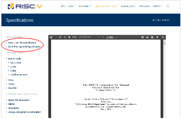
RISC-V Foundation website’s architecture documents
The biggest difference between the RISC-V architecture and other mature commercial architectures is that it is a modular architecture. Thus, the RISC-V architecture is not only concise but also allows different parts to be organized modularly, attempting to meet various applications through a unified architecture.
This modularity is not present in the x86 and ARM architectures. For example, the ARM architecture is divided into three series: A, R, and M, targeting application operating systems, real-time applications, and embedded fields respectively, with no compatibility among them. However, the modular RISC-V architecture allows users to flexibly choose different modules to combine and meet different application scenarios, making it suitable for all ages. For instance, for small area and low power consumption embedded scenarios, users can choose the RV32IC combination instruction set, using only the machine mode; while for high-performance application operating system scenarios, they can choose instruction sets like RV32IMFDC, utilizing both machine mode and user mode.
The concise architecture and modular philosophy make the number of instructions in the RISC-V architecture very simple. The basic number of RISC-V instructions is only over 40, and with the addition of various modular extended instructions, the total number of instructions is only a few dozen. Figure 2-2 is a diagram of the RISC-V instruction set; please refer to Appendix A for detailed information on the RISC-V instruction set.
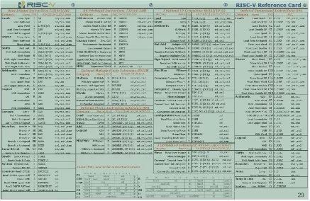
RISC-V Instruction Set Diagram
What Does This Book Cover?
“Hand-in-Hand Guide to CPU Design” provides a systematic and comprehensive introduction to the RISC-V architecture in extremely simple and easy-to-understand language, and combines the open-source processor core of the E200 series with in-depth explanations of CPU design technology, illustrated and lively, reflecting the author’s profound professional skills and excellent ability to present professional knowledge in a popular manner. What is particularly impressive is that during the introduction of the RISC-V architecture, the author includes a wealth of background knowledge interpretation and personal annotations, making the dry professional knowledge very easy to understand; it can be said to be a rare achievement. This book, which condenses the author’s years of learning, is very worthwhile to read, and will have a huge impact on the dissemination of the RISC-V architecture in China. As one of the few Chinese books introducing RISC-V, it is believed to become a classic in this field.
What is the Table of Contents for This Book?
(Slide to view on mobile)
Part One Overview of CPU and RISC-V
Chapter 1 Understanding CPUs in One Article
1.1 Seeing the High-Rise, Seeing the Guests, Seeing the Building Collapse — The Life of CPUs
1.1.1 ISA — The Soul of the CPU
1.1.2 CISC and RISC
1.1.3 32-bit and 64-bit Architectures
1.1.4 The Life of ISAs
1.1.5 Divisions of CPU Domains
1.2 ISA Must Bear This Burden — Why Domestic CPUs Have Not Yet Succeeded Sufficiently
1.2.1 MIPS Series — Loongson and Junzheng
1.2.2 x86 Series — Beijing University of Posts and Telecommunications, Zhaoxin, and Haiguang
1.2.3 Power Series — Zhongsheng Hongxin
1.2.4 Alpha Series — Shenwei
1.2.5 ARM Series — Feiteng, Huawei HiSilicon, Spreadtrum, and Huaxintong
1.2.6 Blame It on ISA
1.3 Life is Already So Difficult, Why Must You Expose It — The Helplessness of CPU Practitioners
1.4 Invincible is So Lonely — The World Dominated by ARM
1.4.1 Solitary Joy and Shared Joy — The Profit Model of ARM
1.4.2 The Small Guy Has Great Power — The Ubiquitous Cortex-M Series
1.4.3 The Mobile King — The Huge Success of Cortex-A Series in Handheld Devices
1.4.4 The Attack on Giants — ARM’s Ambition to Enter the PC and Server Fields
1.5 East Rises with the Sun, West Rains; It is Said to be Sunny but There is Rain — RISC-V is Here
1.6 So You Are This Kind of “Potato Chips” — ARM’s Free Program
1.7 The Former Wang Xie Swallows in Front of the Hall, Flying into the Ordinary People’s Home — You Can Design Your Own Processor
Chapter 2 Simplicity is Beauty — The Soul of RISC-V Architecture
2.1 Simplicity is Beauty — The Design Philosophy of RISC-V Architecture
2.1.1 Light as a Feather — The Length of Architecture
2.1.2 Flexible and Adaptable — Modular Instruction Set
2.1.3 Essence is Concentrated — Number of Instructions
2.2 Introduction to RISC-V Instruction Set Architecture
2.2.1 Modular Instruction Subsets
2.2.2 Configurable General Purpose Register Set
2.2.3 Structured Instruction Encoding
2.2.4 Simple Memory Access Instructions
2.2.5 Efficient Branch Jump Instructions
2.2.6 Simple Subroutine Calls
2.2.7 Unconditional Code Execution
2.2.8 No Branch Delay Slot
2.2.9 Zero-Cost Hardware Loops
2.2.10 Simple Operation Instructions
2.2.11 Elegant Compressed Instruction Subsets
2.2.12 Privileged Modes
2.2.13 CSR Registers
2.2.14 Interrupts and Exceptions
2.2.15 Vector Instruction Subsets
2.2.16 Custom Instruction Extensions
2.2.17 Summary and Comparison
2.3 RISC-V Software Toolchain
2.4 How RISC-V Differs from Other Open Architectures
2.4.1 The People’s Hero — OpenRISC
2.4.2 The Noble — SPARC
2.4.3 The Ivy League — RISC-V
Chapter 3 A Beautiful Mess — Review of RISC-V Commercial and Open Source Versions
3.1 Overview of Commercial and Open Source Versions
3.1.1 Rocket Core (Open Source)
3.1.2 BOOM Core (Open Source)
3.1.3 Freedom SoC (Open Source)
3.1.4 LowRISC SoC (Open Source)
3.1.5 PULPino Core (Open Source)
3.1.6 PicoRV32 Core (Open Source)
3.1.7 SCR1 Core (Open Source)
3.1.8 ORCA Core (Open Source)
3.1.9 Andes Core (Commercial IP)
3.1.10 Microsemi Core (Commercial IP)
3.1.11 Codasip Core (Commercial IP)
3.1.12 E200 Core & SoC (Open Source)
3.2 Summary
Chapter 4 China’s First Open Source RISC-V — E200 Series Ultra-Low-Power Core & SoC
4.1 The Unique E200 Processor
4.2 Introduction to E200 — Small but Complete
4.3 E200 Model Series
4.4 E200 Performance Indicators
4.5 E200 Supporting SoC
4.6 E200 Configuration Options
Part Two Hands-on Guide to Using
Verilog to Design CPU
Chapter 5 Seeing the Forest Before the Trees — Overview and Top-Level Introduction to E200 Design
5.1 Overview of Processor Hardware Design
5.1.1 Architecture and Microarchitecture
5.1.2 CPU, Processor, Core, and Processor Core
5.1.3 Characteristics of Processor Design and Verification
5.2 Design Philosophy of E200 Processor Core
5.3 RTL Code Style of E200 Processor Core
5.3.1 Using Standard DFF Module Instantiation to Generate Registers
5.3.2 Recommended Use of Assign Syntax Instead of If-Else and Case Syntax
5.3.3 Other Considerations
5.3.4 Summary
5.4 Module Hierarchy of E200 Processor Core
5.5 Source Code of E200 Processor Core
5.6 Configuration Options of E200 Processor Core
5.7 Supported RISC-V Instruction Subsets of E200 Processor Core
5.8 Pipeline Structure of E200 Processor
5.9 Introduction to Top-Level Interface of E200 Processor Core
5.10 Summary
Chapter 6 Pipelining is Not a Roster — Introduction to E200 Pipeline
6.1 Overview of Processor Pipeline
6.1.1 Starting from the Classic Five-Stage Pipeline
6.1.2 Is It Possible to Do Without Pipelining? — The Relationship Between Pipelining and State Machines
6.1.3 Deeply Planting Water Chestnuts and Shallowly Planting Rice, Not Deep or Shallow Planting Lotus — The Depth of the Pipeline
6.1.4 Growing Upwards — Increasingly Deeper Pipelines
6.1.5 Growing Downwards — Increasingly Shallower Pipelines
6.1.6 Summary
6.2 Out-of-Order Execution in Processor Pipeline
6.3 Back Pressure in Processor Pipeline
6.4 Conflicts in Processor Pipeline
6.4.1 Resource Conflicts in Pipeline
6.4.2 Data Conflicts in Pipeline
6.5 Pipeline of E200 Processor
6.5.1 Overall Structure of the Pipeline
6.5.2 Conflicts in the Pipeline
6.6 Summary
Chapter 7 Is It Difficult to Start? — Everything Starts with Instruction Fetching
7.1 Overview of Instruction Fetching
7.1.1 Characteristics of Instruction Fetching
7.1.2 How to Fetch Instructions Quickly
7.1.3 How to Handle Misaligned Instructions
7.1.4 How to Handle Branch Instructions
7.2 Simplification of Instruction Fetching by RISC-V Architecture Characteristics
7.2.1 Structured Instruction Encoding Format
7.2.2 Instruction Length Indicator Placed in Low Bits
7.2.3 Simple Branch Jump Instructions
7.2.4 No Branch Delay Slot Instructions
7.2.5 Providing Clear Static Branch Prediction Basis
7.2.6 Providing Clear RAS Basis
7.3 Instruction Fetching Implementation of E200 Processor
7.3.1 Overall Design Ideas of IFU
7.3.2 Mini-Decode
7.3.3 Simple-BPU Branch Prediction
7.3.4 PC Generation
7.3.5 Accessing ITCM and BIU
7.3.6 ITCM
7.3.7 BIU
7.4 Summary
Chapter 8 One Shot, Execution is Key — Execution
8.1 Overview of Execution
8.1.1 Instruction Decoding
8.1.2 Instruction Execution
8.1.3 Conflicts in Pipeline
8.1.4 Delivery of Instructions
8.1.5 The Order of Instruction Dispatch, Execution, and Write Back
8.1.6 Branch Resolution
8.1.7 Summary
8.2 Simplification of Execution by RISC-V Architecture Characteristics
8.2.1 Structured Instruction Encoding Format
8.2.2 Elegant 16-Bit Instructions
8.2.3 Simplified Number of Instructions
8.2.4 Integer Instructions are All Two-Operand
8.3 Execution Implementation of E200 Processor
8.3.1 Execution Instruction List
8.3.2 Overall Design Ideas of EXU
8.3.3 Decoding
8.3.4 Integer General Purpose Register Set
8.3.5 CSR Registers
8.3.6 Instruction Dispatch and Execution
8.3.7 Pipeline Conflicts, Long Instructions, and OITF
8.3.8 ALU
8.3.9 High-Performance Multiplication and Division
8.3.10 Floating Point Unit
8.3.11 Delivery
8.3.12 Co-processor Extensions
8.3.13 Summary
Chapter 9 Starting is Difficult — Delivery
9.1 Overview of Processor Delivery, Cancellation, and Flushing
9.1.1 Introduction to Processor Delivery, Cancellation, and Flushing
9.1.2 Common Implementation Strategies for Processor Delivery
9.2 Simplification of Delivery by RISC-V Architecture Characteristics
9.3 Hardware Implementation of E200 Processor Delivery
9.3.1 Handling of Branch Prediction Instructions
9.3.2 Handling of Interrupts and Exceptions
9.3.3 Delivery of Multi-Cycle Execution Instructions
9.4 Summary
Chapter 10 Let the Bullets Fly for a While — Write Back
10.1 Overview of Processor Write Back
10.1.1 Introduction to Processor Write Back Function
10.1.2 Common Strategies for Processor Write Back
10.2 Hardware Implementation of E200 Processor Write Back
10.2.1 Final Write Back Arbitration
10.2.2 OITF and Long Instruction Write Back Arbitration
10.2.3 Summary
Chapter 11 The Most Unnoticeable is Actually the Most Difficult — Memory Architecture
11.1 Overview of Memory Architecture
11.1.1 Who Says Processors Must Have Cache
11.1.2 Processors Must Have Memory
11.1.3 ITCM and DTCM
11.2 Simplification of Memory Access Instructions by RISC-V Architecture Characteristics
11.2.1 Only Supporting Little Endian Format
11.2.2 No Address Increment/Decrement Mode
11.2.3 No “Read Multiple Data at Once” and “Write Multiple Data at Once” Instructions
11.3 Memory-Related Instructions of RISC-V Architecture
11.3.1 Load and Store Instructions
11.3.2 Fence Instructions
11.3.3 “A” Extension Instructions
11.4 Hardware Implementation of Memory Subsystem of E200 Processor
11.4.1 Overall Design Ideas of Memory Subsystem
11.4.2 AGU
11.4.3 LSU
11.4.4 ITCM and DTCM
11.4.5 Handling of “A” Extension Instructions
11.4.6 Handling of Fence and Fence.I Instructions
11.4.7 BIU
11.4.8 ECC
11.4.9 Summary
Chapter 12 The Window of the Black Box — Bus Interface Unit BIU
12.1 Overview of On-Chip Bus Protocol
12.1.1 AXI
12.1.2 AHB
12.1.3 APB
12.1.4 TileLink
12.1.5 Summary Comparison
12.2 Custom Bus Protocol ICB
12.2.1 Introduction to ICB Bus Protocol
12.2.2 ICB Bus Protocol Signal
12.2.3 ICB Bus Protocol Timing
12.3 Hardware Implementation of ICB Bus
12.3.1 One Master, Multiple Slaves
12.3.2 Multiple Masters, One Slave
12.3.3 Multiple Masters, Multiple Slaves
12.4 BIU of E200 Processor Core
12.4.1 Introduction to BIU
12.4.2 BIU Microarchitecture
12.4.3 BIU Source Code Analysis
12.5 SoC Bus of E200 Processor
12.5.1 Introduction to SoC Bus
12.5.2 SoC Bus Microarchitecture
12.5.3 SoC Bus Source Code Analysis
12.6 Summary
Chapter 13 A Story That Must Be Told — Interrupts and Exceptions
13.1 Overview of Interrupts and Exceptions
13.1.1 Overview of Interrupts
13.1.2 Overview of Exceptions
13.1.3 Broadly Defined Exceptions
13.2 Exception Handling Mechanism of RISC-V Architecture
13.2.1 Entering an Exception
13.2.2 Exiting an Exception
13.2.3 Exception Service Routine
13.3 Interrupt Definitions in RISC-V Architecture
13.3.1 Types of Interrupts
13.3.2 Interrupt Masking
13.3.3 Interrupt Waiting
13.3.4 Interrupt Priority and Arbitration
13.3.5 Interrupt Nesting
13.3.6 Summary Comparison
13.4 Exception-Related CSR in RISC-V Architecture
Registers
13.5 Hardware Implementation of Exception Handling in E200 Processor
13.5.1 Key Points of Exception and Interrupt Implementation in E200 Processor
13.5.2 Types of Exceptions in E200 Processor
13.5.3 Handling of mepc in E200 Processor
13.5.4 Interrupt Interface of E200 Processor
13.5.5 Microarchitecture and Source Code Analysis of CLINT in E200 Processor
13.5.6 Microarchitecture and Source Code Analysis of PLIC in E200 Processor
13.5.7 Delivery Module of E200 Processor’s Handling of Interrupts and Exceptions
13.5.8 Summary
Chapter 14 The Most Unnoticeable is Actually the Most Difficult — Debugging Mechanisms
14.1 Overview of Debugging Mechanisms
14.1.1 Overview of Interactive Debugging
14.1.2 Overview of Tracing Debugging
14.2 Debugging Mechanism of RISC-V Architecture
14.2.1 Implementation of Debugger Software
14.2.2 Debugging Mode
14.2.3 Debugging Instructions
14.2.4 CSR for Debugging Mechanisms
14.2.5 Debugging Interrupts
14.3 Hardware Implementation of Debugging Mechanisms in E200 Processor
14.3.1 Overview of Interactive Debugging in E200
14.3.2 DTM Module
14.3.3 Hardware Debugging Module
14.3.4 Handling of Debugging Interrupts
14.3.5 Implementation of CSR Registers for Debugging Mechanisms
14.3.6 Implementation of Debugging Mechanism Instructions
14.4 Summary
Chapter 15 Moving Like a Rabbit, Staying Still Like a Maiden — Secrets of Low Power Consumption
15.1 Overview of Low Power Consumption Techniques for Processors
15.1.1 Low Power Consumption at Software Level
15.1.2 Low Power Consumption at System Level
15.1.3 Low Power Consumption at Processor Level
15.1.4 Low Power Consumption at Unit Level
15.1.5 Low Power Consumption at Register Level
15.1.6 Low Power Consumption at Latch Level
15.1.7 Low Power Consumption at SRAM Level
15.1.8 Low Power Consumption at Combinational Logic Level
15.1.9 Low Power Consumption at Process Level
15.2 Low Power Consumption Mechanisms of RISC-V Architecture
WFI Instruction
15.3 Hardware Implementation of Low Power Consumption Mechanisms in E200
15.3.1 System-Level Low Power Consumption in E200
15.3.2 Processor-Level Low Power Consumption in E200
15.3.3 Unit-Level Low Power Consumption in E200
15.3.4 Register-Level Low Power Consumption in E200
15.3.5 Latch-Level Low Power Consumption in E200
15.3.6 SRAM-Level Low Power Consumption in E200
15.4 Summary
Chapter 16 To Do a Good Job, One Must Sharpen One’s Tools — RISC-V Expandable Co-Processors
16.1 Domain-Specific Architectures (DSA)
16.2 Expandability of RISC-V Architecture
16.2.1 Reserved Instruction Encoding Space in RISC-V
16.2.2 Predefined Custom Instructions in RISC-V
16.3 Co-Processor Interface EAI of E200
16.3.1 Encoding of EAI Instructions
16.3.2 EAI Interface Signals
16.3.3 EAI Pipeline Interface
16.3.4 EAI Memory Interface
16.3.5 Timing of EAI Interface
16.4 Reference Example of Co-Processor in E200
16.4.1 Example Co-Processor Requirements
16.4.2 Example Co-Processor Instructions
16.4.3 Example Co-Processor Implementation
16.4.4 Example Co-Processor Performance
16.4.5 Example Co-Processor Code
Part Three Using Verilog for Simulation and Running Software on FPGA SoC Prototypes
Chapter 17 Just a Puff of Smoke — Running Verilog Simulation Tests
17.1 Code Hierarchy Structure of E200 Open Source Project
17.2 Test Cases of E200 Open Source Project
17.2.1 riscv-tests Self-Test Cases
17.2.2 Compiling ISA Self-Test Cases
17.3 Test Platform of E200 Open Source Project (TestBench)
17.4 Running Test Cases in Verilog TestBench
Chapter 18 Putting on a Shell and Hitting the Road — Implementing SoC and FPGA Prototypes
18.1 Introduction to Freedom E310 SoC
18.2 Introduction to HBird-E200-SoC
18.2.1 Composition Structure of HBird-E200-SoC
18.2.2 Code Structure of HBird-E200-SoC
18.3 FPGA Prototype Platform for HBird-E200-SoC
18.3.1 FPGA Development Board
18.3.2 Generating mcs Files for FPGA Burning
18.3.3 JTAG Debugger
18.3.4 DIY FPGA Prototype Platform
Summary
18.4 Dedicated FPGA Development Board for E200
Chapter 19 The Finishing Touch — Running and Debugging Software Examples
19.1 Introduction to Freedom-E-SDK Platform
19.2 Introduction to SIRV-E-SDK Platform
19.2.1 Introduction to SIRV-E-SDK
19.2.2 Code Structure of SIRV-E-SDK
19.3 Running Example Programs Using SIRV-E-SDK
19.4 Debugging Examples Using GDB and OpenOCD
19.5 Windows Graphical IDE Development Tools
Chapter 20 Is It a Mule or a Horse? Take It Out for a Walk — Running Benchmark Programs
20.1 Introduction to Benchmark Programs
20.2 Introduction to Dhrystone
20.3 Running Dhrystone Benchmark
20.4 Introduction to CoreMark
20.5 Running CoreMark Benchmark
20.6 Summary and Comparison
Appendix A Introduction to RISC-V Architecture Instruction Set
Appendix B Introduction to RISC-V Architecture CSR Registers
Appendix C Introduction to RISC-V Architecture PLIC
Appendix D Background Introduction to Memory Models
Appendix E Background Introduction to Memory Atomic Operation Instructions
Appendix F RISC-V Instruction Encoding List
Appendix G RISC-V Pseudo Instruction List