The basic workflow of the energy-saving lighting controller can be further refined as follows: 1) Collecting ambient light intensity data: The system obtains real-time ambient light intensity through a light sensor. As the ambient light changes, the light sensor continuously outputs new light intensity data. 2) Data processing and analysis: The main control chip (for example, STC89C51) is responsible for collecting and processing the light intensity data output from the light sensor, filtering it, performing algorithmic processing, and extracting valid data that meets the requirements. At the same time, the system continuously collects information about the ambient light intensity. 3) Controlling output signals and controlling the light switch: The calculated valid data is converted into control signals, which are output to the LED driver circuit through hardware circuits, controlling the brightness and switch state of the LED lights. As the light intensity increases, the brightness of the LED lights decreases, ensuring both lighting quality and energy-saving effects. 4) Displaying system status information: The system can also display the current time and ambient light intensity information on an LCD screen to help users intuitively understand the current lighting status and ambient light conditions. Overall, the energy-saving lighting system obtains ambient light intensity data through a light sensor, processes and analyzes the data through the main control chip, and outputs the calculated control signals to the LED lights to control their brightness and switch state, thereby achieving energy-saving and emission reduction goals. The basic workflow diagram is shown below.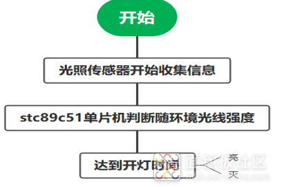 1. Minimum System of STC89C51 MicrocontrollerThe main function of the control microcontroller is to execute and control external loops. We used a minimum system board based on the STC89C51 chip. We only need to call the I/O pin code to achieve input and output functions on the system board. The working voltage of the computer is 12V, which can collect input data from other modules and output it to other communication modules.Therefore, the implementation of the energy-saving lighting system is realized because the main STC89C51 minimum system board is the core part of the entire energy-saving lighting system design, controlling the input and output of data for each module and the working status of each module. The following minimum system of the microcontroller is shown in the figure below, suitable for the minimum system board in STC89C51.
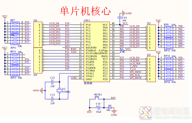 2. OLED Display Module Circuit DesignThis solution uses a 0.96-inch black and white OLED display based on IIC communication, with a maximum resolution of 128*64. This OLED display has an SSD1306 driver chip as the display driver chip and also includes a voltage regulator chip to maintain stable voltage.The screen also has a freely luminous viewing angle, allowing values on the screen to be observed from multiple angles. This OLED display is a screen based on IIC communication, and the circuit connection is as follows: The circuit connection method of the 0.96-inch OLED module is generally divided into the following steps: 1) Interface description: A typical 0.96 OLED module usually has I2C or SPI interfaces. I2C is a serial communication protocol based on two wires (SDA and SCL), supporting multiple devices to communicate on the same bus; while SPI is a serial communication protocol with a chip select signal. 2) VCC pin and GND pin: Connect the module’s VCC pin to the positive power supply and the GND pin to the negative power supply for power supply. 3) The I2C interface connection method of the OLED module is as follows: – Connect the module’s SCL pin to the MCU’s I2C clock line (i.e., SCL) – Connect the module’s SDA pin to the MCU’s I2C data line (i.e., SDA). – If multiple I2C devices are configured in hardware, the module’s address pin needs to be connected to VCC/GND/NC based on specific conditions. 4) The SPI interface connection method of the OLED module is as follows: – Connect the module’s CS pin to a programmable GPIO pin. – Connect the module’s DC pin to a programmable GPIO pin. – Connect the module’s SCLK pin to the MCU’s SPI clock line. – Connect the module’s SDIN pin to the MCU’s MOSI line. After setting its parameters and program, it will automatically reset when powered on after power off. The low power consumption of the OLED display also helps reduce system power consumption. The core SSD1306 driver chip can perform page addressing mode or horizontal and vertical addressing mode operations.The addressing method determines how data is written. Using the IIC interface for communication, the OLED display module has: the VCC pin can connect to 3.3V voltage, the GND pin is the negative power supply of the display screen that can be grounded, the SCL pin manages the clock signal of IIC communication controlled by the computer program to communicate with the display screen, and the SDA pin is the data transmission pin used in IIC communication, with a total of four pin interfaces corresponding to the OLED’s D1 pin (this design connects to the GPIOA0 pin of the STM32F103C8T6 microcontroller);The OLED display module is one of the important ways for the system to interact with users in home security systems. Users can understand the changes in environmental data in real-time through the data displayed on the OLED screen, converting analog data into visual data. Therefore, the OLED display module is an important component of the home security system, and the schematic diagram of the OLED display module is shown below:
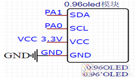 3. Light Sensor Circuit DesignFirst, the photoresistor is a component that changes its resistance value according to the intensity of light. When designing the light sensor circuit, the photoresistor needs to be the core component. Secondly, the basic principle of the light sensor circuit is to connect the photoresistor in series with other components of the circuit to form a feedback circuit. When light shines on the photoresistor, the resistance value of the photoresistor changes according to the intensity of the light, thereby affecting the working state of the entire circuit. Finally, to ensure that the light sensor circuit can work normally, it is necessary to reasonably configure other components, such as capacitors, diodes, etc. In addition, to reduce noise interference in the circuit, suitable filters and amplifiers should also be selected during the design process.When the ambient light changes, the voltage value at the sensor interface pin will also change accordingly, adapting to the light intensity. At the same time, the sensitivity can be adjusted through the potentiometer in the sensor module. After the voltage signal output from the sensor is amplified by the operational amplifier, accurate measurement results can be obtained. The photoresistor sensor module is suitable for scenarios that require automatic control to measure and respond to ambient light.For example, motion control and indoor lighting, etc. In addition, it is also widely used in industrial automation, machine vision, and other fields. For instance, in industrial automation, it can be used to measure the position of items, and machines can utilize its sensitivity to measure the color and brightness characteristics of object surfaces. In summary, the photoresistor module is easy to use and provides reliable measurement results, making it one of the core sensors in the field of automatic control. The light sensor circuit is shown in the figure below.
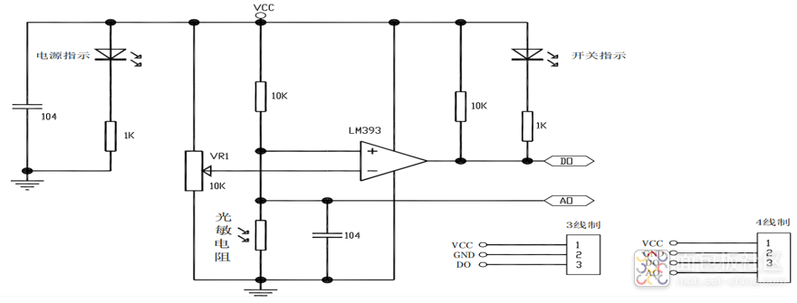 4. Indicator Light ModuleThe indicator light module is a small device that can emit light, mainly used in circuits to indicate whether the circuit is functioning normally and whether the status is normal. The commonly used indicator light module usually consists of several basic parts, including a bulb, a resistor, and some connecting wires.The circuit connection is as follows: The VCC pin and IN are connected to the positive power supply, and the GND pin is connected to the ground. When the circuit is functioning normally, the indicator light module lights up and emits bright light, while when there is a fault or abnormality in the circuit, the indicator light module does not light up. Thus, we can know whether the circuit is normal by observing the status of the indicator light module, ensuring the normal operation of the equipment.In addition to being used in circuits, the indicator light module can also be widely applied in various machines, devices, and automobiles, making it more convenient for us to understand the status of the equipment. The indicator light module has been widely used in production, manufacturing, and technology fields, and its application range is continuously expanding, with more developments expected in the future. The circuit diagram of the indicator light module is shown below.
 5. EEPROM MemoryThe EEPROM memory module is a programmable memory that differs from traditional ROM memory, allowing data to be erased and programmed through electrical signals, making data reading and modification more convenient and flexible.The circuit connection is as follows: VCC and GND pins: Connect the chip’s VCC pin to the positive power supply and the GND pin to the negative power supply; A0, A1, A2 address pins: Select the enabled address pins to be grounded or connected to a high level as needed to determine the chip’s address; WP pin: This pin can be used for write protection control. If write protection is needed, connect it to the negative power supply; if write protection is not needed, connect it to the positive power supply; SDA, SCL bus pins: Connect the chip’s SDA pin to the MCU’s I2C data bus and the SCL pin to the MCU’s I2C clock bus. The EEPROM memory module consists of a storage unit array, control logic, and I/O interfaces, among which the storage unit array is the most critical part, mainly composed of a series of field-effect transistors and metal-oxide semiconductors that form the storage units, allowing charges to be stored in the dielectric layer to achieve data storage functionality.The control logic is mainly responsible for command decoding, address detection, data input and output, and various functions, playing a crucial role in implementing the functions of the EEPROM memory module. The I/O interface is used for data exchange between the EEPROM memory module and external devices, containing multiple bits and other control pins for reading and writing data in the memory. The EEPROM memory module has various advantages such as electrically erasable, programmable, and readable, and is widely used in data storage and processing of various electronic devices. The schematic diagram of the EEPROM memory is shown below.
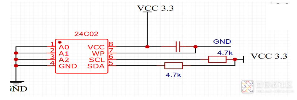 6. DS1302 Clock ModuleThe DS1302 is an SPI interface real-time clock module that can continuously count and provide slope compensation functionality. This module integrates a crystal compensation circuit, which helps stabilize the clock frequency and improve clock accuracy. The DS1302 is a real-time clock module based on the SPI interface, featuring continuous counting and slope compensation functionality, with a built-in crystal compensation circuit to enhance clock accuracy.The circuit connection of the DS1302 module uses the SPI interface for communication, which has four pins: VCC, GND, RST, SLCK, and IO. Among them, VCC is the power pin, GND is the ground pin, RST is the reset pin, and IO is the data input/output pin. SLCK connects to the clock signal. The circuit diagram of the DS1302 clock module is shown below.
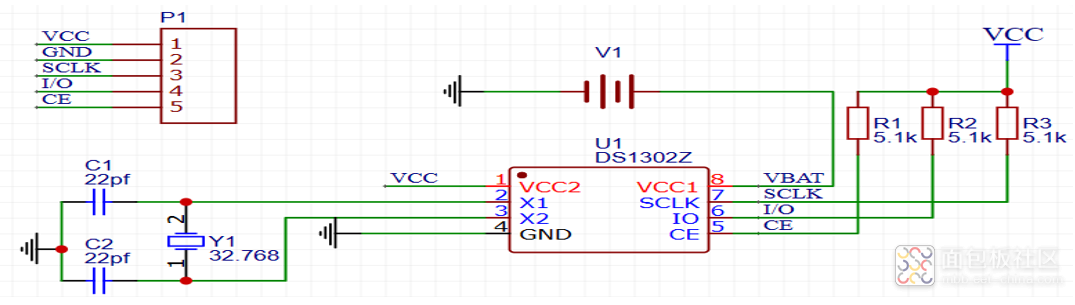 7. OLED Display Code 1) Initialize the I2C bus: First, the IIC bus in the 51 microcontroller needs to be initialized, including the settings of the SCL and SDA pins, clock frequency, and other parameters. The following is the core code of this system design:
#define SCL P2_0 // Define SCL pin#define SDA P2_1 // Define SDA pinvoid I2C_Init(){ SCL = 1; // Set SCL to high SDA = 1; // Set SDA to high}2) Sending the I2C start signal: When using the I2C communication protocol for data transmission, a start signal must first be sent, which is a pulse that pulls down the SDA pin for a longer duration on the bus. The following is the core code of this system design:
void I2C_Start(){ SDA = 1; SCL = 1; SDA = 0; // Send start signal SCL = 0;}3) Sending the I2C stop signal: After writing data to the OLED, an I2C stop signal must be sent to end the data transmission. The following is the core code of this system design:
void I2C_Stop(){ SDA = 0; SCL = 1; SDA = 1; // Send stop signal}4) Writing commands or data: When writing data or commands, the corresponding control byte and data byte must be sent according to the I2C communication protocol. The following is the core code of this system design:
void I2C_WriteByte(unsigned char dat){ unsigned char i = 0; for (i = 0; i < 8; i++) { SDA = (dat & 0x80) >> 7; dat <<= 1; SCL = 1; SCL = 0; } SDA = 1; SCL = 1; SCL = 0;}5) Reading data: When reading data from the OLED, it must be done according to the I2C communication protocol, and the data read is saved to a specified address. The following is the core code of this system design:
unsigned char I2C_ReadByte(){ unsigned char i, dat = 0; SDA = 1; for (i = 0; i < 8; i++) { dat <<= 1; SCL = 1; dat |= SDA; SCL = 0; } return dat;}Note:This article is reproduced from the Breadboard Community We will handle any copyright issues, please contact the author if there are any questions!Submission/Recruitment/Advertisement/Course Cooperation/Resource Exchange, please add WeChat: 13237418207, and note “Join Group” to pull you into the official technical WeChat group of Fan Yi Education, to communicate technical issues and insights with other electronics experts~

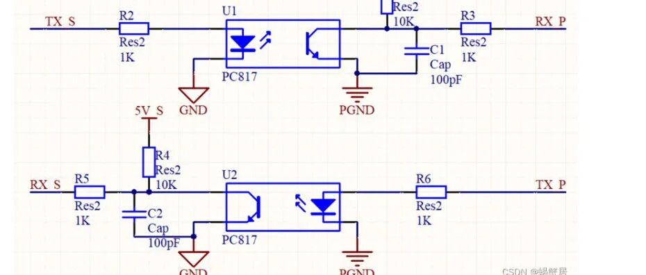
Serial isolation circuit, a copy without a sound
PCB design suggestions for DDR module circuits

Scan to add customer service WeChat, note “Join Group” to pull you into the official technical WeChat group of Fan Yi Education, to communicate technical issues and insights with other electronics experts~
Share 💬 Like 👍 Follow ❤️ Support!