
Abstract

Digital phase-locked amplifiers are widely used in various scientific fields for high-resolution measurements. Experimental evidence shows that due to the additional 1/f noise observed at the output of the phase-locked amplifier, current state-of-the-art commercial models cannot measure signals with a resolution better than tens of ppm. This noise arises from low-frequency gain fluctuations experienced by the signal from the generation stage to the acquisition stage. To overcome these fluctuations, we conceived and implemented a novel switching ratio architecture that achieves noise suppression, with performance experimentally validated, improving the resolution by more than an order of magnitude (from 9 ppm to 0.6 ppm). This paper describes the implemented mixed-signal board (named ELIA, Enhanced Lock-In Amplifier) and discusses several important design details for maximizing the resolution of the phase-locked amplifier.
Keywords
Phase-locked amplifier; sub-ppm resolution; high frequency; FPGA
Contact: Xiao Lu
Phone: 13693671247
Scan to join:
Phase-Locked Amplifier Technical Exchange Group 1
Phase-Locked Amplifier Technical Exchange Group 2
Gathering of experts, waiting for you!

1. Introduction
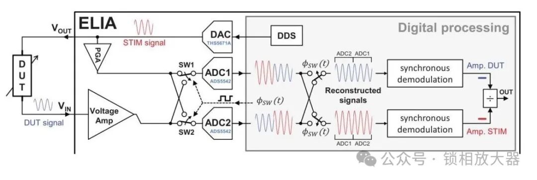
Phase-locked amplifiers (LIAs) are powerful instruments used to detect and measure periodic signals in the presence of significant noise. Due to their combined advantages of flexibility, cost, and performance, digital phase-locked amplifiers are becoming increasingly popular in many experimental setups [1]. The resolution of these instruments, defined as the minimum detectable change in the input signal, is typically expected to be set by the equivalent input noise of the acquisition channel. Specifically, the resolution should be determined by the input range of the instrument and is independent of the amplitude of the input signal. However, the measured resolution of fast digital lock-in instruments can be in the tens of ppm, several orders of magnitude worse than expected [2]. In particular, the demodulated signal at the output of the phase-locked amplifier exhibits unexpected additional 1/f noise, which is proportional to the signal amplitude and nearly independent of the frequency of the input signal. Regardless of the measurement bandwidth, the output 1/f noise limits the resolution of the lock-in instruments. We found that this signal-proportional 1/f noise is due to gain fluctuations experienced by the signal during the generation and acquisition stages. These fluctuations are primarily caused by the fast digital-to-analog (D/A) and analog-to-digital (A/D) converters used in digital phase-locked amplifiers [3]. Although the gain fluctuations may be slower compared to the signal frequency fAC, they randomly modulate the signal amplitude. Since the coherent detection of the phase-locked amplifier extracts the amplitude of the signal at fAC, the output of the phase-locked amplifier maintains random fluctuations similar to the gain. Here, we report the design and preliminary experimental results of a digital phase-locked amplifier specifically designed to eliminate these fluctuations. Figure 1 shows the conceptual scheme of the instrument. Detailed theoretical discussions will be reported elsewhere [3]. In brief, the input signal from the device under test (DUT) and the generated (or stimulus) signal (STIM) are both acquired and processed in parallel by the instrument to compute their amplitudes. The gain fluctuations are eliminated through a ratio operation between the two amplitudes. To be effective, although acquiring both signals simultaneously requires two different analog-to-digital converters (ADCs), the DUT and STIM signals must experience the same gain fluctuations. To achieve this, the two ADCs alternately acquire the DUT and STIM signals through two switches SW1 and SW2 inserted before the ADCs. A field-programmable gate array (FPGA) is used to reconstruct the signals in real-time to continuously obtain their temporal evolution in the digital domain. As in standard phase-locked amplifiers, the amplitudes (and phases) of the two signals are calculated through quadrature demodulation. The switching frequency fSW of SW1 and SW2 is chosen to be in the hundreds of Hz, which is faster than the slow random gain fluctuations of the instrument. Therefore, the equivalent gain experienced by the two reconstructed signals within one period 1/fSW is the same and equals the average gain of the two ADCs. The input DUT signal and the acquired STIM signal are both affected by the same gain fluctuations of the analog-to-digital converter (ADC) and digital-to-analog converter (DAC), thus ideally canceling each other out in the final ratio operation.
The following sections describe the design of the analog and digital electronics of the implemented instrument. Section 4 reports the experimental validation of the digital phase-locked amplifier.

2. Hardware Design
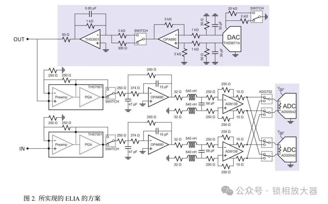
The implemented Enhanced Lock-In Amplifier (ELIA) instrument includes a generation channel, two acquisition channels, and an FPGA digital core. Figure 2 shows the hardware scheme. The components that compensate for gain fluctuations through the switching ratio technique are highlighted in blue.

2.1 Generation Channel
The voltage generation channel produces an output sine wave signal with a maximum frequency of 20 MHz and an amplitude selectable between 50 µV and 10 V. It includes a digital-to-analog converter (DAC) and a driver stage. The selected DAC is Texas Instruments (TI) 14-bit resolution, high-speed (up to 125 MS/s, operating here at 80 MS/s), low-power model THS5671A. A switch allows selection between two different reference resistors to set the full-scale output current range of the ADC (20 mA or 2 mA). The next stage converts the differential output current signal of the DAC into a single-ended voltage signal. Then, an output driver stage is implemented, allowing selection between two possible gains via a second switch. This way, the output can be adjusted to three possible ranges (100 mV, 1 V, and 10 V when driving high impedance). Unlike the two acquisition channels, the generation channel does not require special attention to reduce gain fluctuations. In fact, since the DUT and STIM signals are shared, all gain fluctuations are compensated through the ratio technique (blue parts in Figure 2).
2.2 Acquisition Channels
The acquisition part includes two identical channels for the DUT and STIM signals. The first stage amplification is implemented by TI’s single-chip THS7001, which includes a high input impedance preamplifier providing 6 dB of gain and low 1.7 nV/√Hz voltage noise, followed by a digitally controlled programmable gain amplifier (PGA) providing a -22 dB to 20 dB attenuation/gain range. After this first conditioning stage, a 4th order 20 MHz Butterworth anti-aliasing filter is implemented. The first pair of complex conjugate poles is obtained through a Sallen-Key architecture, while the second pair is obtained through a passive RLC filter. A fast (400 MHz bandwidth, G=1) differential operational amplifier (Analog Devices’ AD8139) converts the signal from single-ended to differential, setting a 1.55 V common-mode voltage required by the subsequent ADC. Before the two ADCs, a network composed of four single-pole double-throw switches (Analog Devices’ ADG752) allows precise selection of the two differential signals to be alternately connected to one of the two 14-bit, 80 MS/s ADCs (TI’s ADS5542 model), as discussed later. The switching ratio technique allows compensation for gain fluctuations in the stages after the switches. Therefore, it may be useful to place the switches as the first stage of the acquisition channel. However, in this initial implementation, we decided to place them before the ADC for two reasons: i) the main source of gain fluctuations is the ADC; ii) due to the fast differential operational amplifier and switches, the samples after switching SW1 and SW2 can be correctly acquired. If the switches were placed as the first stage, the last condition would not be satisfied due to the settling time of the anti-aliasing filter.
2.3 Design Details for Reducing Gain Fluctuations
As mentioned earlier, the switching ratio technique can compensate for the slow gain fluctuations of the digital-to-analog converter (DAC), signal generation chain, and analog-to-digital converter (ADC), with the fluctuations of the ADC being the most significant. However, to break through the resolution limit, it is also crucial to reduce the gain fluctuations of uncompensated components. These components are located in two independent acquisition paths, from the preamplifier to the switches. Here, the DUT and STIM signals are processed separately, and the gain fluctuations are uncorrelated, thus cannot be eliminated through ratio operations. Specifically, the components that need to be considered include: i) resistors involved in the channel transfer function; ii) programmable gain amplifiers (PGAs); iii) switches before the ADC.
To minimize the impact of resistors, we used non-standard metal foil resistors produced by Vishay Precision Group, which have a low temperature coefficient (≤0.2 ppm/K) and low inherent 1/f noise [4].
Temperature fluctuations can cause the gain of the PGA to vary with a gain temperature coefficient of about 25−35 ppm/K. Since this value is quite large, we implemented a bypass path to verify whether it would lead to a decrease in resolution. Experimental results showed that when both PGAs were not bypassed, performance slightly degraded (from 0.6 to 0.85 ppm). However, it is worth noting that some chips contain two PGAs with good inter-channel gain temperature coefficient matching (a few ppm/K) [5]. This feature will be considered in future implementations, as the correlated fluctuations between the two acquisition channels can be compensated through ratio operations.
For the switch network, the voltage divider formed by the switch resistance and the finite differential input resistance of the ADS5542 ADC, which has a resistance of RADC ≈ 6.6 kΩ, needs to be considered. The random fluctuations of the ADC input resistance itself are not an issue, as the technique can compensate for their effects. Instead, the switch resistance may vary independently, leading to uncorrelated fluctuations in the two voltages acquired by the ADC. To reduce their impact, we chose switches with low resistance (RSW = 15 Ω). This way, their fluctuations will have a reduced impact on the transfer function of RSW/(RSW + 15 Ω + RADC) ≈ 0.0023 times.
3. Digital Architecture
The digital core of the implemented ELIA is a Xilinx Spartan 6 FPGA (installed on the commercial module Opal Kelly XEM6010, which also includes a phase-locked loop, external memory, and USB interface). The implemented digital architecture includes:
• Direct digital frequency synthesizer (DDS) for generating phase and quadrature sine signals;
• DAC and ADC control interface module;
• Signal reconstruction module;
• Multipliers for phase and quadrature demodulation;
• Filters, decimators, and dividers;
• A PC interface module.
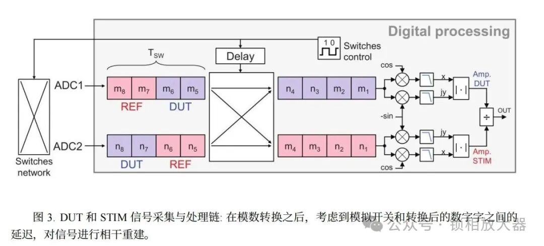
To implement the switching ratio technique, the only additional modules required compared to a standard dual-channel phase-locked amplifier (LIA) are the reconstruction module and the final divider. The reconstruction module (Figure 3) simply takes the signals from the two ADCs and coherently places them into the DUT and STIM digital processing chains. A delay module is used to set the correct timing for signal reconstruction.
4. Results
The ELIA instrument has been manufactured (Figure 4) and has passed experimental validation. As an example of its performance, Figure 5(a) shows the tracking of a time-varying resistance of 250 Ω, which varies periodically by ∆R = 1.25 mΩ (i.e., 5 ppm). Measurements were conducted under three different conditions: (1) using Zurich Instruments’ commercial advanced HF2LI; (2) using the custom ELIA as a standard phase-locked amplifier (i.e., measuring only the DUT signal); (3) using the ELIA with the switching ratio technique (fSW = 1 kHz). The signal amplitude applied to the time-varying resistor was 300 mV, with a filter bandwidth of 1 Hz. For the HF2LI, the obtained resolution was 39 ppm; the resolution of the ELIA used as a standard phase-locked amplifier was 9 ppm; and the resolution of the ELIA using the proposed technique was 0.6 ppm. The resolution improved by more than an order of magnitude (from 9 ppm to 0.6 ppm), allowing for clear detection of small (5 ppm) resistance modulation steps. Similar resolution (<0.8 ppm) was also achieved using complex impedance as the DUT, indicating that this operation is insensitive to signal phase and measurement frequencies up to 6 MHz.
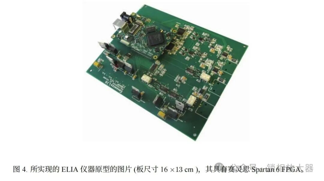
Figure 5(b) shows the instrument output noise spectrum obtained under the same experimental conditions. Specifically, we kept the amplitude of the generated signal and the external DUT unchanged, but to obtain a wider spectrum, we varied the filter bandwidth (BW = 1 kHz), lock-in frequency (fac = 100 kHz), and the frequency of the instrument’s switch network (fSW = 2 kHz). We removed the 48 MΩ resistor as it was not significant for assessing noise performance. These spectra confirm the performance improvement, as expected, with a significant reduction in 1/f noise compared to standard implementations.


5. Conclusion
A novel phase-locked architecture can compensate for low-frequency gain fluctuations of the digital-to-analog converter (DAC) and analog-to-digital converter (ADC), which typically limit the resolution of instruments. This technique requires the implementation of a second acquisition channel (identical to the first channel and sometimes already present in commercial instruments) before the two ADCs, as well as a switch network. From the perspective of the digital architecture, only a few additional modules need to be easily implemented in the FPGA. To fully leverage this architecture for sub-ppm resolution, careful consideration must be given to the design of uncompensated stages, or it may degrade resolution performance. In particular, non-standard resistors, temperature-stable programmable gain amplifiers (PGAs), and the correct selection of ADC switches need to be used. The implemented ELIA serves as a high-resolution alternative to standard phase-locked amplifiers, such as in sensor or device characterization applications, without the need to change experimental setups or perform calibrations.
<img src=”https://mmbiz.qpic.cn/mmbiz_jpg/vOHfvyeiaVEQ9utA30UxGg4GGTjyLYaHq5qnvVaibMCGCIrTQfqLEvG1xqicia6OspBH1AzWvNK10iaV5E5yL7zJVQ/640?wx_fmt=jpeg&from=appmsg&watermark=1″