Problem Statement
Dear Zhu, I recently encountered a problem that I would like to consult you about. We are using the OPA2350 for our electromagnetic operational amplifier, and instead of copying a board, I designed a circuit myself. The waveform simulated in Multisim is correct, and the rectified waveform is also correct; when I tested the circuit I soldered, the rectified output waveform was fine, showing a very stable high level. However, when I connected this output to the ADC input of the microcontroller, the waveform changed to a triangular wave shape!
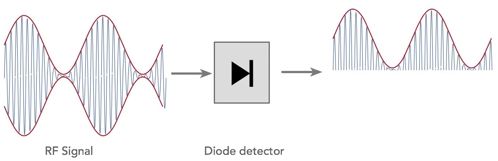
Signal Diode Detection Schematic
Initially, I thought there was an issue with the program, but when I directly connected a high level to the ADC input of the microcontroller, the waveform and collected values were correct and unchanged. So now I am very confused about where my circuit went wrong; I have been struggling with this for four days. I hope you can help me analyze where the problem might be. Thank you!
Principle Explanation
The issue above is actually due to the linear attenuation and nonlinear distortion caused by the internal resistance of the signal source and the load impedance during the transmission of the electrical signal between circuit systems. The solution is quite simple, which will be provided later. However, let’s take this opportunity to explore more diverse solutions behind this problem together.
1. Signal Detection and Demodulation
Using an E-shaped inductor (typically a 10mH inductor paired with a 6.2nF capacitor) to sense the alternating magnetic field information on the track, the magnitude of the signal is related to the position of the inductor on the track. To simplify, let’s assume the inductor’s direction remains horizontal and parallel to the normal of the track; the output induced voltage p(x,y) only relates to the position.
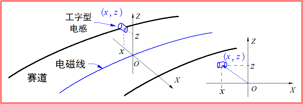
Electromagnetic Navigation Inductor Position
The voltage signal V(t) obtained after signal amplification is represented in the following diagram:
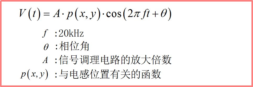
Mathematical Expression of Received Signal
From this, we can see that the signal is essentially an amplitude-modulated signal modulated by positional information. Therefore, to obtain the actual p(x,y) signal, we need to demodulate the amplitude-modulated signal. Of course, how to derive the position of the inductor from p(x,y) is another issue to be discussed later.
Signal modulation and demodulation were initially topics of interest for radio enthusiasts, but for students studying automation, this issue may be relatively unfamiliar. However, this method of processing signals indeed holds an important position in signals and systems. Let’s delve into this topic.
There are two main categories for demodulating ordinary amplitude-modulated signals: one is synchronous demodulation, and the other is envelope detection. Both methods are introduced in courses on signals and systems or radio communications, so we won’t elaborate on them here.
Next, we will derive mathematically and provide more ways to demodulate signals.
2. Phase Demodulation
If we can obtain a signal V(t) that is phase-shifted by 90°, then calculating the modulus of the corresponding real and imaginary parts of these two signals will yield the demodulated signal. Specifically, it is shown in the following formula:
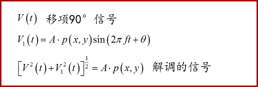
Phase Demodulation Principle
For general signals, a 90° phase shift can be achieved using the Hilbert transform. The signal and its Hilbert transform together form a complex number known as the analytic signal of that signal. The modulus of the analytic signal equals the envelope of the signal. This content belongs to advanced signal processing methods, and due to space limitations, we will skip the 5000-word description.
For actual electromagnetic signals, phase-shift demodulation can be performed through ADC sampling using a microcontroller. By sampling at two adjacent times T, or sampling the signal itself and its delayed version, as long as T is an integer multiple of the carrier period plus a quarter or three-quarters of the period, the two sampled signals will differ by 90° in phase. Calculating their root mean square will yield the demodulated signal.
3. Nonlinear Demodulation
If we examine the square term of the V(t) signal, we can see that there are two components in the result:
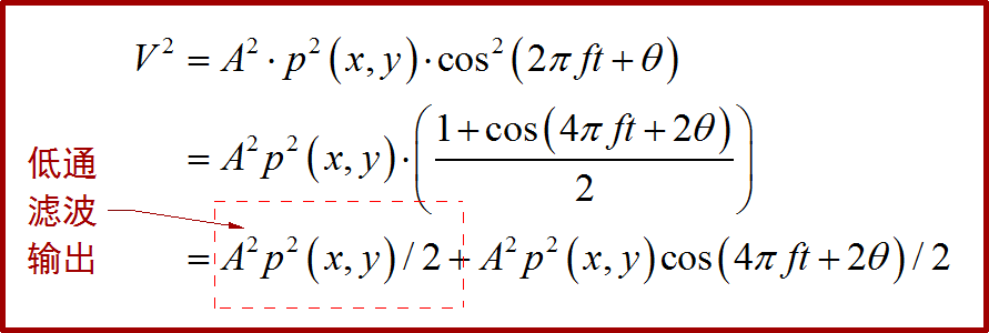
Square of Amplitude-Modulated Signal Contains Low-Frequency Information
One component is the low-frequency part of the unmodulated signal, while the other is the double-frequency modulated signal. Therefore, by using a low-pass filter, we can obtain the low-frequency signal, and then demodulate it to retrieve the original signal.
To implement the square operation on the signal, we can use hardware analog multipliers or perform calculations in software after ADC conversion. Additionally, passing the signal through any nonlinear element can also yield the square term of the signal. According to the Taylor series expansion of functions, we can see that at least the quadratic term of the series contains the square term of the signal.
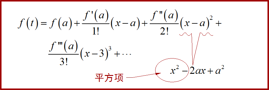
Taylor Series Expansion of Nonlinear Transfer Function
Thus, by passing the signal through a nonlinear element and then applying a low-pass filter, we can obtain the low-frequency part of the signal to be demodulated, and further processing such as removing constants, appropriately taking square roots, and multiplying can recover the modulated signal.
In electronic circuits, common electronic components such as diodes, transistors, and operational amplifiers are actually nonlinear components. If these components are combined with resistive and capacitive elements to form a signal amplification circuit, it is necessary to set the correct operating point and feedback to achieve linear amplification as much as possible. However, if they are used for signal demodulation, the circuit design needs to be intentionally made nonlinear. Therefore, a poorly designed amplification circuit may score only 10 points in an ordinary analog electronics course, but in signal demodulation, it could be an excellent circuit that earns 100 points.
4. Nonlinear Demodulation Circuits
(1) Diode Detection Circuit
Utilizing the unidirectional conduction characteristic of diodes can form a diode envelope detection circuit. The subsequent resistor and capacitor work with the diode to complete the charging and discharging, ultimately obtaining the envelope signal of the amplitude-modulated wave at the circuit output.
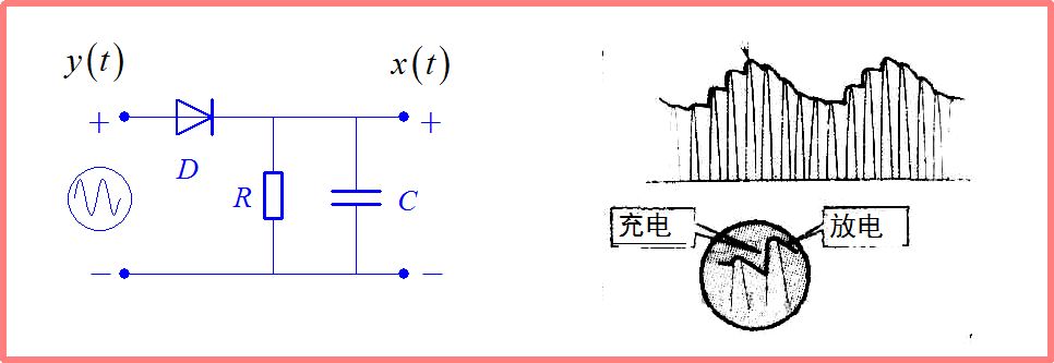
Diode Detection Circuit
The above process is overly simplistic and corresponds to the detection process of high amplitude signals. In practice, diodes have characteristics such as conduction voltage, forward resistance, and reverse leakage current, which cause significant losses for weak high-frequency signals during detection, and may even fail to complete detection. Furthermore, this detection method has weaknesses such as high output impedance and low load capacity.
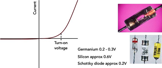
Diode Transfer Characteristics and High-Frequency Diodes
Methods to improve the detection of weak high-frequency signals include:
-
Using germanium diodes or Schottky diodes with lower conduction voltages;
-
Applying appropriate bias to the diodes;
-
Using voltage doubling detection;
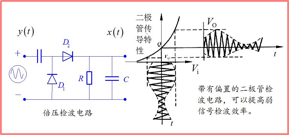
Two Methods to Improve Detection Efficiency: Voltage Doubling Detection and Bias Detection
If we want to further increase detection efficiency, we can use transistors to complete the detection.
(2) Transistor and MOS Detection Circuit
Utilizing the nonlinearity of transistors and MOS under small bias can achieve signal detection. It is equivalent to a biased diode detection + transistor amplification circuit, so this detection method is more efficient, with greater gain and lower output impedance. The following diagram shows a two-stage MOS and BJT high-frequency detection circuit.
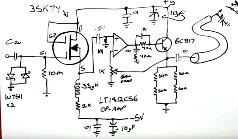
Transistor Detection Circuit
(3) Operational Amplifier Detection Circuit
Setting the operational amplifier’s operating point to the critical cutoff state can also achieve detection of amplitude-modulated signals. This circuit can simultaneously amplify and detect the signal, with low output impedance.
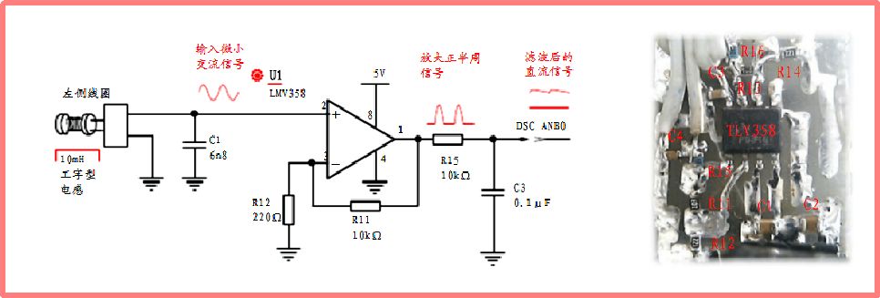
Operational Amplifier Detection Circuit
The above circuit is excerpted from the electromagnetic vehicle model design guide published by the competition committee.
Problem Analysis
For different detection circuits, the output impedance and filtering methods vary. The main reasons for the initial problem posed by the student are:
-
When signals are transmitted in actual systems, the internal resistance of the output system and the input impedance of the signal input port must be considered;
-
The internal resistance of the signal source changes significantly with the amplitude of the output signal, especially for weak signals, where the output impedance of the diode detection is very high;
-
The values of R and C in the detection circuit greatly affect the output signal waveform, often requiring the product of RC to correspond to a time constant that is several times greater than the carrier period T.
The time constant of the detection circuit also needs to consider the impact of the load. If the load resistance is small, it will likewise reduce the time constant, resulting in significant fluctuations in the output waveform.
Most I/O ports of ordinary microcontrollers are multiplexed with various functions, so the ADC input port may have pull-up or pull-down bias resistors from the original I/O port. If the MCU port function is improperly set, it may reduce the impedance of the ADC input port.
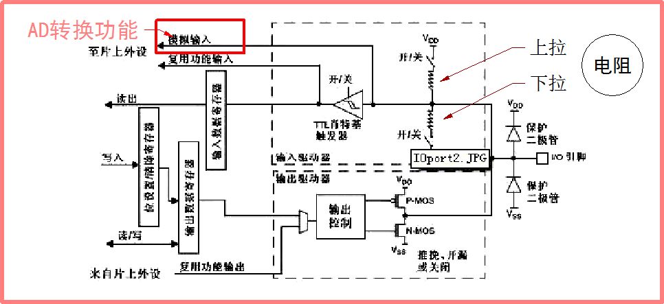
MCU Composite Port Internal Circuit Schematic
Therefore, the primary reason for the waveform becoming unsmooth after the diode detection when connected to the ADC input of the MCU is likely due to the ADC input port being opened with a bias resistor, reducing the input resistance and affecting the filtering time constant of the detection circuit.
Hardware Solutions:
-
Set the MCU’s ADC input port to a high-impedance state;
-
Increase the capacitor C in the diode detection circuit and increase the R value, so that the filtering time length reaches several ms, which is dozens of times the carrier period of 20kHz.
-
Add a voltage follower between the rectification circuit and the ADC to isolate the impact of the MCU’s ADC input resistance on the detection circuit;
-
Replace with integrated circuit nonlinear detection to improve the load capacity of the detection circuit.
Software Solutions:
Based on the previously introduced phase-shift detection method, hardware signal detection may not be necessary; instead, the amplified amplitude-modulated signal can be directly sent to the ADC after level shifting, using software to calculate the signal envelope.
Experimental Verification
Experiment 1: Results from the Student’s Experiment.
Dear Zhu, you just mentioned that improper settings of the ADC port could cause the problems I described. I just tested it, and adding a voltage follower perfectly solved my issue.
Besides adding a voltage follower, are there other ways to solve this problem? Is the improper setting of the ADC conversion port an issue with the internal design of the chip? If it is a problem with the ADC conversion settings, then why does using the 386 not require a voltage follower and still does not encounter the issues I mentioned?
For answers to the subsequent questions, please refer to the solutions provided in the principle explanation.
Experiment 2: Phase Shift Detection of Signals
This experiment is derived from the previous discussion on ultrasonic signal navigation (input “beacon navigation” in the public account to find this post) regarding the demodulation of ultrasonic signals.
The frequency of the ultrasonic wave is 40kHz, and the sampling frequency is 53.33kHz. The period used is equal to three-quarters of the signal carrier period, so the two adjacent sampling data differ by -90° (270°) in the carrier phase. Therefore, calculating the root mean square of the two adjacent sampling data can yield the signal envelope.
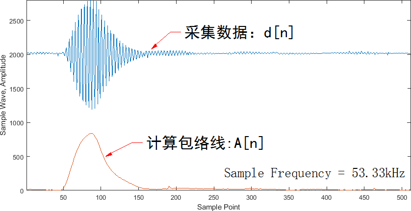
Phase Shift Detection Data
From the above figure, it can be seen that the calculated envelope perfectly reproduces the modulated signal.
Note that in this experiment, data collection needs to first subtract the average DC signal from the ADC conversion.
Experiment 3: Voltage Doubling Detection Circuit
This is a detection circuit for high-frequency signals, which is essentially a voltage doubling detection circuit.
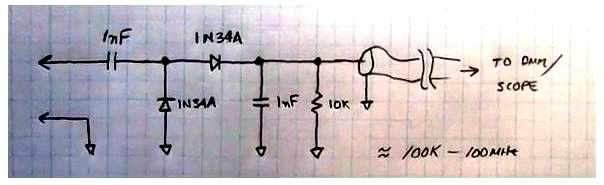
Voltage Doubling Detection Circuit Schematic
To accommodate high-frequency signals, the entire circuit is made very compact, with all components finally housed in a metal shielding box.
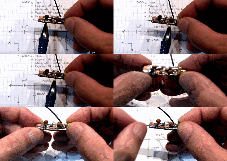
Actual Appearance of the Voltage Doubling Detection Circuit
The entire circuit can maintain detection performance across a wide frequency range. Due to the influence of the diode’s conduction voltage, when the input signal is very weak (less than a few tens of millivolts), the output detection voltage is low. However, when the input signal amplitude exceeds 100mV, the input-output relationship of the detector shows a good correlation.
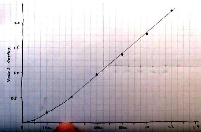
Input-Output Relationship Curve of the Voltage Doubling Detection Circuit
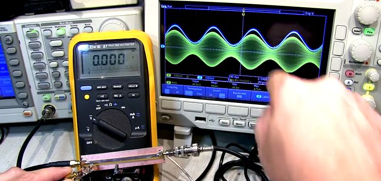
Voltage Doubling Detection Circuit Used for Demodulating High-Frequency Amplitude-Modulated Signals
Summary and Extension
This article primarily discusses the mathematical principles and basic schemes of signal demodulation, while the initial problem encountered by the student pertains to the basic issues of signal transmission in circuits. Different conditions and methods affect the transmission characteristics of the signal. The factors affecting engineering implementation are multifaceted, and it is essential to grasp the essence of the problem through experimentation.
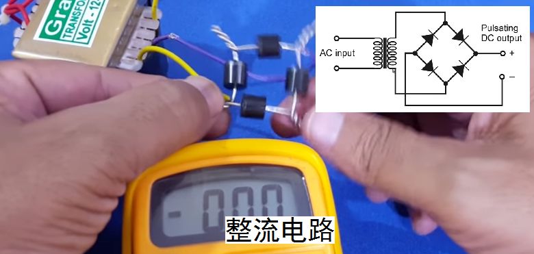
Signal detection is somewhat analogous to signal rectification. However, in AC-DC power conversion, the focus is more on high-voltage, high-current low-frequency power signals, where full-wave bridge rectification is often used to improve system efficiency. In signal detection, due to the weak high-frequency nature of the signals, half-wave or voltage doubling rectification is employed to enhance detection output efficiency. Coupled with subsequent filtering circuits, further separation of the DC and high-frequency signals mixed in the output signal can be achieved.
Signal modulation and demodulation are fundamental signal processing methods. Once the basic principles are understood, signals can be processed through various hardware circuits or software algorithms, leveraging their respective advantages in different contexts.
In practice, it is important for everyone to summarize the experiences gained and further reflect on the underlying principles, so that we can go further in future learning and practice. If anyone wants to learn more about the principles behind the process of making intelligent vehicles, please feel free to ask better questions.

Signals can undergo transformations, and a person’s image can also change. The photo below shows my wife and me transformed to the old Shanghai Bund during the May Fourth Movement.