Documenting the debugging process of a frontend engineer involved in the 2.5GHz A72 backend:
A fellow from the 2.5GHz A72 training camp asked: What are these PBUF_DATA? What is PBUF_CLK? Are all IO PORT BUF called this? Why should they be deleted?
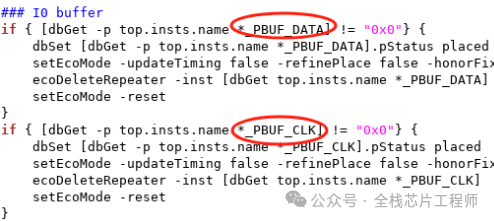
Answer: The IO buffer was added in the synthesis script, so the backend needs to first delete the IO buffer and then re-add the buffer.
A fellow from the training camp asked: There is no port named *_PBUF_CLK in the maia_cpu core’s IO PORT?
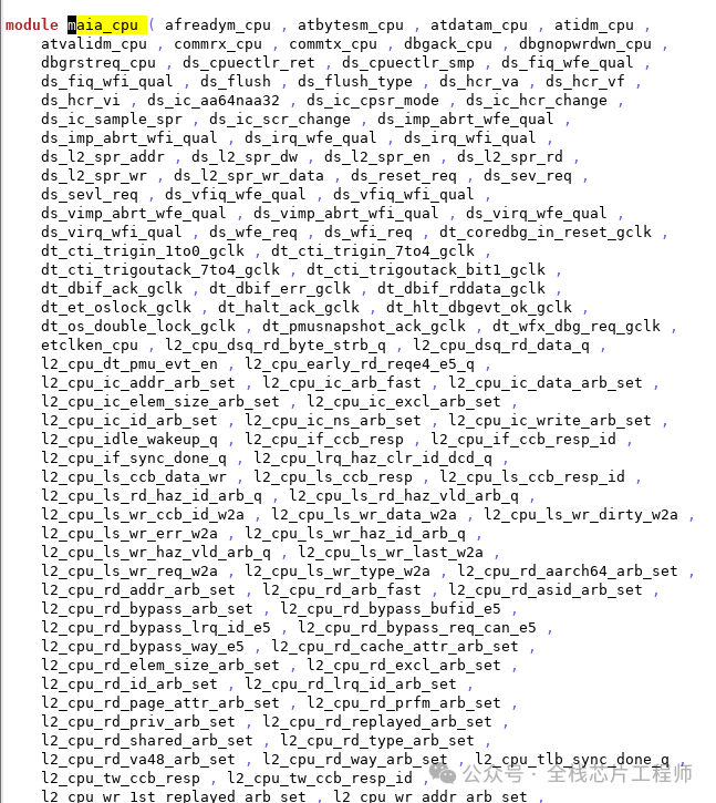
Answer: We can obtain *_PBUF_DATA using the dbGet command, as follows:
dbGet [dbGet -p top.insts.name *_PBUF_DATA].name
In fact, the command we use for adding BUF in synthesis is uniformly named *_PBUF_DATA.

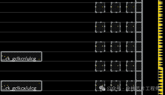
The re-added IO BUFFER is as follows, for more content, refer to the training camp project:
“ 2.5GHz frequency, 12nm process, DVFS low power A72 backend training ”
01
2.5GHz 12nm DVFS A72 backend practical training
1) According to low power requirements, write UPF verification UPF
Master hierarchy UPF file writing, master Flatten UPF file writing.
This project uses hierarchy UPF to divide 7 power domains, voltage domains, specifying power switch cells, including SWITCH TRICKLE, SWITCH HAMMER. Master the use of low power cells, choose appropriate isolation cells, level shifters, and other low power cells.
Master Power gating, Clock gating design techniques.
Master Multi-VT design techniques, this project’s clock tree uses ULVT, with low dynamic power and small skew.
Master DVFS technology, ss0p9 2.5GHz, ss0p72 2.0GHz, where sram does not support ss0p63. If you want to do ss0p63, just give sram vddm a separate 0p7v power supply.
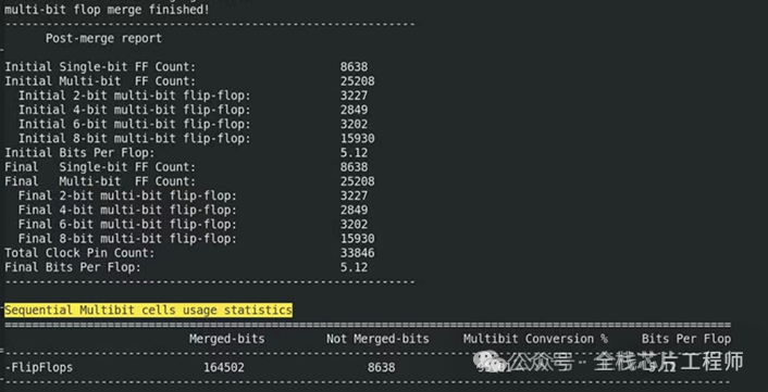
Master the use of multibit cells, in this project, the CPU contains up to 95% mb, selecting appropriate multibit cells to achieve ultra-high CPU utilization. Generally, INNOVUS does not perform mb merge and split. Therefore, the synthesis generally performs multibit merge split.
2) According to top floorplan def, perform CPU subsystem partition and pin assignment.
Top‘s Power stripe planning and push down.
SpecifyBlackBox, mirror partition of CPU core.
Master the method of manual manual cut the BlackBox, mastering the experience of complex floorplan design methods.
VerifyPowerDomain, check the correctness of low power division and UPF.
Pin assignment, arrange pin layout reasonably according to timing requirements, and solve congestion issues.
Master Timing budget.
Master the use of Mixplace for practical CPU automatic floorplan, mastering the AI floorplan methodology.
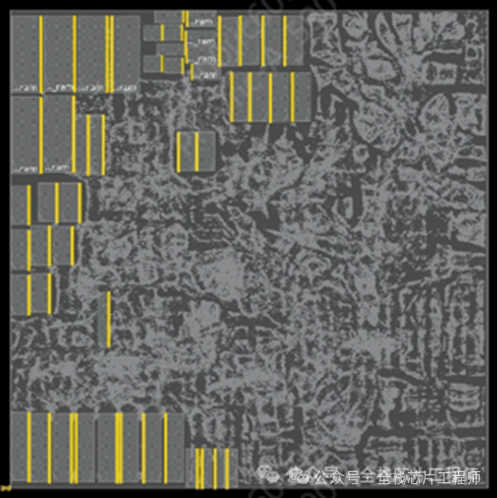
3) Master Fusion compiler DCG, use fusion compiler to complete DCG synthesis, further optimizing timing and congestion.
4) Master the design methodology of hierarchy ICG, practically understanding the significant impact of setting or not setting key ICG on timing.
5) Master Stapling technology, practically mastering the layout and special routing methodology of power switch cells, mastering the powerplan planning and implementation of the CPU subsystem, ensuring the alignment of the CPU subsystem and the top-level PG.
6) Master the timing interface optimization of the CPU subsystem and TOP. Master the placement of TOP isolation cells and the electrical characteristic checks of isolation cell inputs.
7) Master the optimization processing of clock tree Balance for TOP and CPU subsystems, handling common clock paths. Clock tree structure trace and clock tree evaluation.
8)DRC/LVS
DRC/LVS check of the CPU subsystem
DRC/LVS check of the TOP system
Hierarchy & Flatten LVS check principles and implementation methods
9) Static timing analysis &IR-Drop
DMSA flow
Establish PT environment according to Foundry‘s SOD (signoff doc) Timing signoff standards.
Star RC parasitic extraction and related item checks
Timing exception analysis, including set_false_path, set_multicyle_path analysis.
PT timing signoff hierarchical and Flatten Timing checks
PT and PR timing differences analysis, Dummy insertion and with dummy Timing analysis
IR-Drop analysis
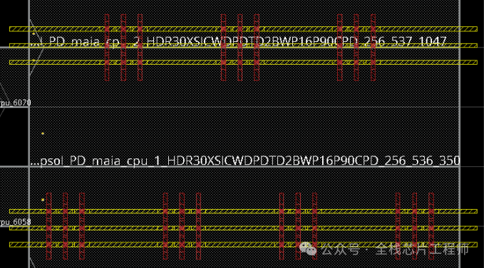
Stampling is truly a high-level manual art, unique online:
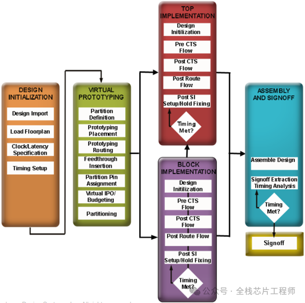
Flow: Partition Flow
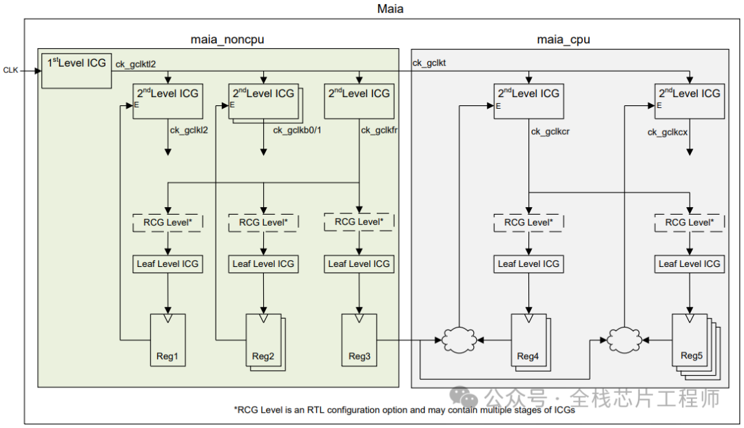
Clock structure analysis:
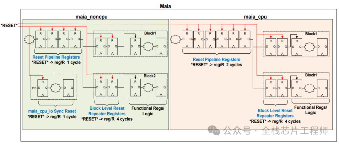
Redundancy structure analysis:
The 12nm 2.5GHz A72 practical training camp requires special settings for Latency, the TOP structure is as follows. Students who have participated in the Jingxin SoC full process training camp know that we will manually instantiate ICG to control the clock in the CRG part, for specific implementation refer to the 40nm Jingxin SoC full process training project. This article introduces the Latency background of the 12nm 2.5GHz A72 practical training camp, welcome to join the practice.
Clock propagation delay Latency, often referred to as insertion delay. It can be divided into two parts: clock source insertion delay (source latency) and clock network delay (Network latency).
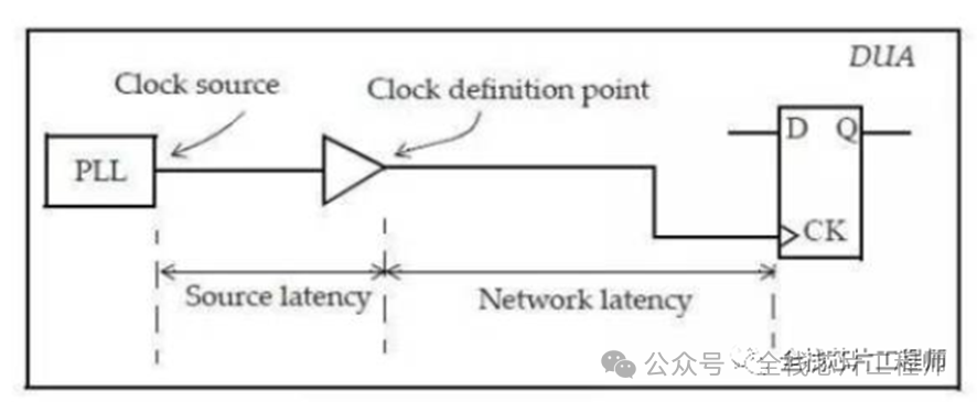
Most training camp students usually set Latency to 0 directly, so what is the use of the latency value? In fact, this is equivalent to a target value, the CTS engine will insert buffers based on the latency value you set to achieve your latency target value.
The following figure is divided into 1st Level ICG and 2nd Level ICG, why are these ICGs divided into two layers?
Why not set all Latency to 0? How much should the latency of the 2nd Level ICG be set?
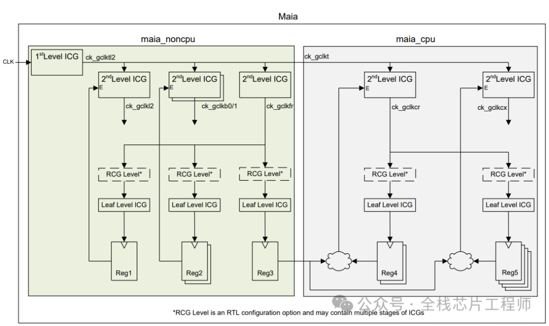
The size of latency directly affects the calculation of clock skew. The clock tree is aimed at balance; assuming a latency value of 400ps is set for a root and sink, then for another sink, even if no latency value is given, CTS will also set the other sink to a latency of 400ps to achieve a smaller skew. Why do we need to create a short clock tree? Because excessive latency values are greatly affected by factors such as OCV and PVT, and there is a presence of time derate.
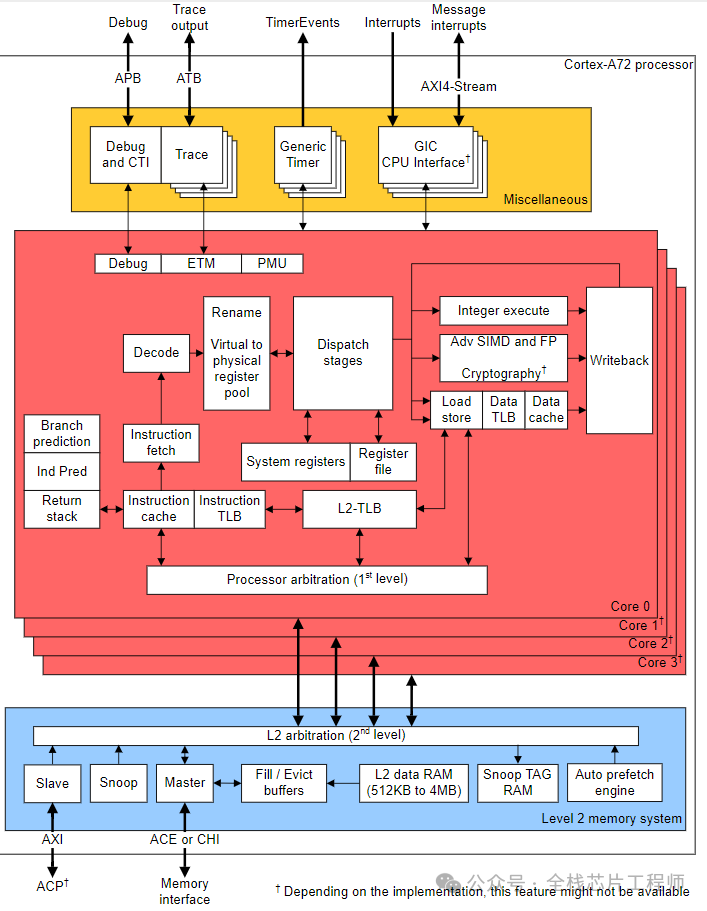
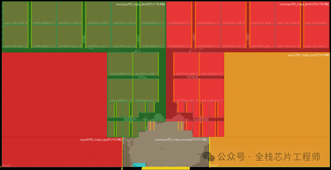
Here’s an example: for low power design of Cortex-A72, why is the isolation of the DBG domain powered by VDDS_maia_noncpu instead of the TOP’s VDD?
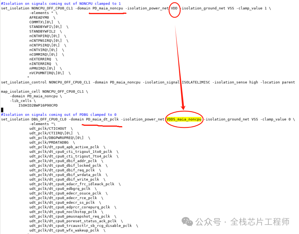
Answer: Because the upper level of dbg is noncpu, and noncpu is divided into dbg and two tbnk.
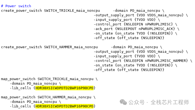
Again, here’s an example: Cortex-A72 low power design, is this switch cell a dual switch? Answer: No, the division of trickle and hammer is to solve the hash current large current problem, first open trickle, then open hammer.
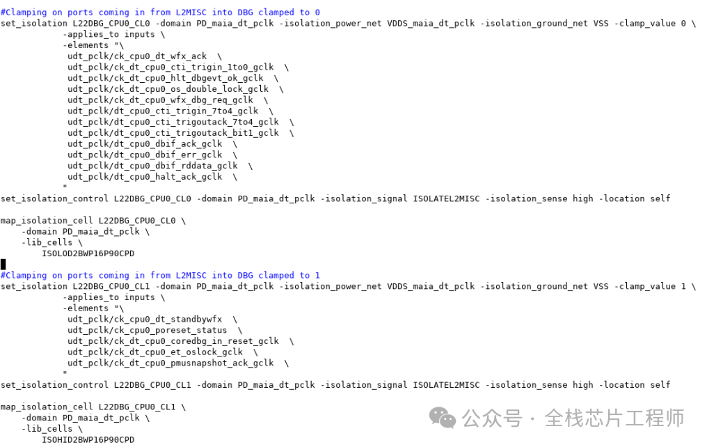
Again, here’s an example: for the advanced version course of Cortex-A72, regarding low power examples: If the iso cell outputs are all to be placed on the parent and inputs on self, then why is the location corresponding to -applies_to_outputs below self?
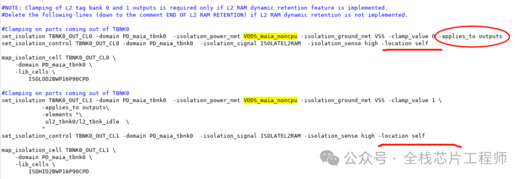
Answer: This requires understanding the internal design architecture of the CPU; if tbnk is powered down, VDDS_maia_noncpu will also inevitably be powered down, as follows, so -applies_to_outputs corresponding to -location can be accepted, then pay attention to the debug domain?

In fact, there are no signals from tbnk to the debug domain, so the script is as follows:
Again, here’s an example: for the advanced version course of Cortex-A72 regarding low power examples: why are the VDD and VDDM of non_cpu SRAM connected to a power supply that can be turned off? The VDD and VDDM of SRAM are normally open and retention power supplies, right?
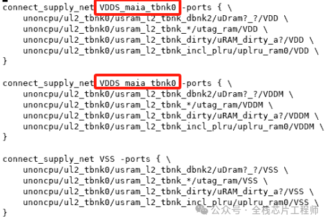
Answer: Originally, VDDM was designed as a retention power supply. After VDD is turned off, VDDM can still supply power for retention use, but here we did not do dual power for memory, using SRAM as a single power supply; otherwise, SRAM cannot be completely powered off.
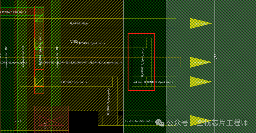
Again, here’s an example: Cortex-A72 basic version course has students whose Cortex-A72 maia_cpu LVS passed , but the top level LVS comparison failed. Let’s locate the issue.
Taking FE_OFN4326_cfgend_cpu1_o as an example, click on the image belowFE_OFN4326_cfgend_cpu1_o:
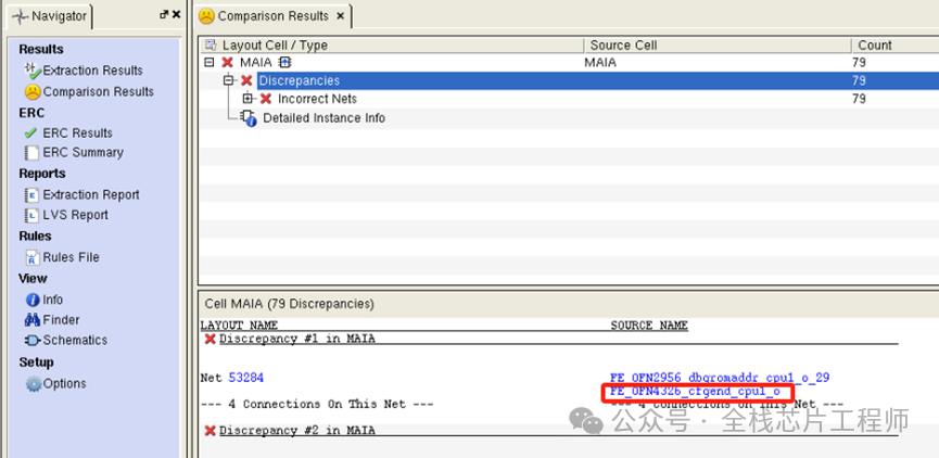
Find the calibredrv error coordinates: (1949,139)
Corresponding to innovus to check the coordinates: (1949,139)
See that the maia_cpu‘s pin is too dense, causing the top-level connection to the pin to be unable to route, leading to innovus routing from the maia_cpu, forming a short. Although the maia_cpu has a blockage, invs does not have enough routing resource to connect the pin, so it can only try to route on maia_cpu.
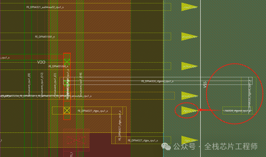
The solution is simple, for specific operations refer to the knowledge star.
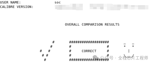
Save the db, re-LVS, comparison passed.
02
28nm Cortex-A7 backend practical training
In addition, we offer the lowest price for 28nm A7 backend design online, with surprising prices! Crushing the backend training prices of 15,000-25,000!
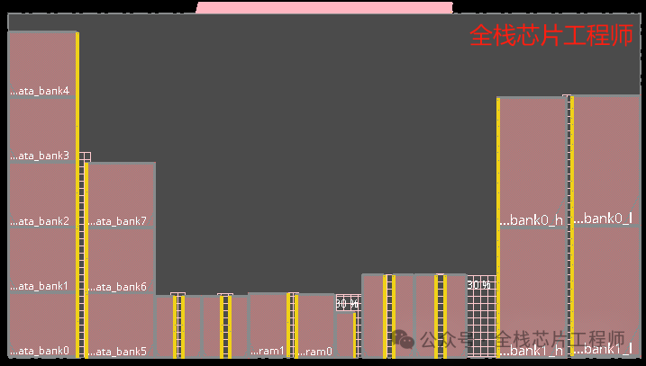
Cortex-A72 single core:
Gates = 240291 Cells = 118421
Cortex-A72 single core:
Gates = 3125649 Cells = 12077666
28nm Cortex-A7 single core:
12nm Cortex-A72 single core:
Area = 486100.9 um2
The 28nm A7 backend design course is promoted at the lowest price in the country, this article will not elaborate too much, the focus of this article is on the advanced 12nm A72 advanced version course.
03
12nm Cortex-A72—DFT practical training
Development completed, lowest price nationwide!
04
Jingxin SoC—Full Chip UPF Backend Practical Training
The full chip UPF low power design (including DFT design) training of Jingxin SoC
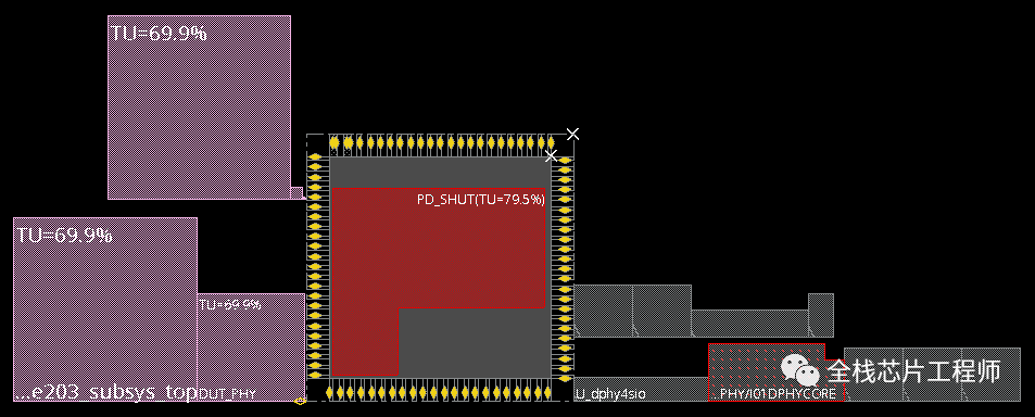
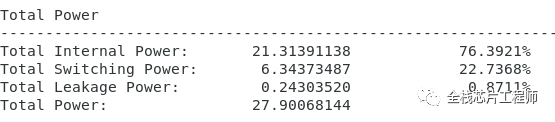
The Jingxin SoC training camp project, before low power design, the power consumption was 27.9mW.
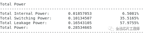
After low power design, the power consumption was 0.285mW, a reduction of 98.9%!
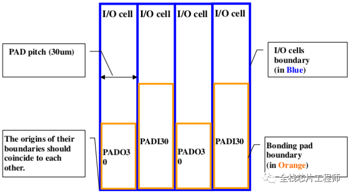
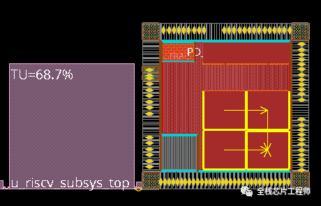
In the 7-day sprint PR training camp, some students asked why some students finished quickly with the same floorplan, while others encountered many DRC issues (EDA tools continuously iterating), causing the tool to never finish running. What specific issues are there?
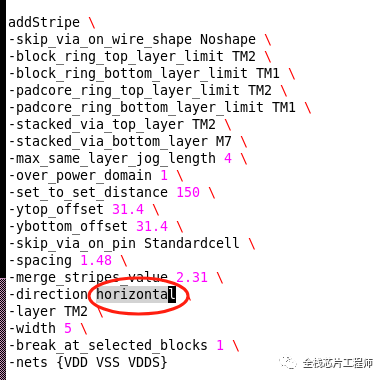
First, the editor found that the stripe of this student defined TM2 as horizontal, while students familiar with Jingxin technology know that the preference direction of TM2 is VERTICAL.
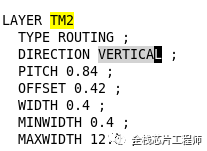
Checking Jingxin’s lef library file can also confirm:
What impact does using the wrong direction have? Everyone should practice in the Jingxin SoC backend flow to gain true knowledge.
In the 7-day sprint PR training camp, some students asked why PR took a whole day and night (24 hours) to complete routing yet still had many DRC errors? The editor has minimized the design scale to speed up PR design, but in fact, routing can be completed in 2 hours; why is it so slow? The reason is the routing of low power cells. For specific reasons and solutions, welcome to join the Jingxin training camp for discussion.
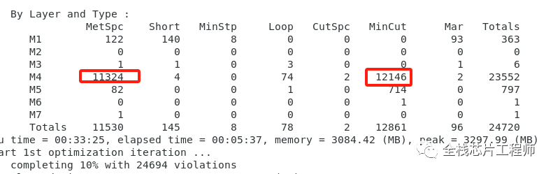
The errors are mainly concentrated on M4, please think about how to solve it.
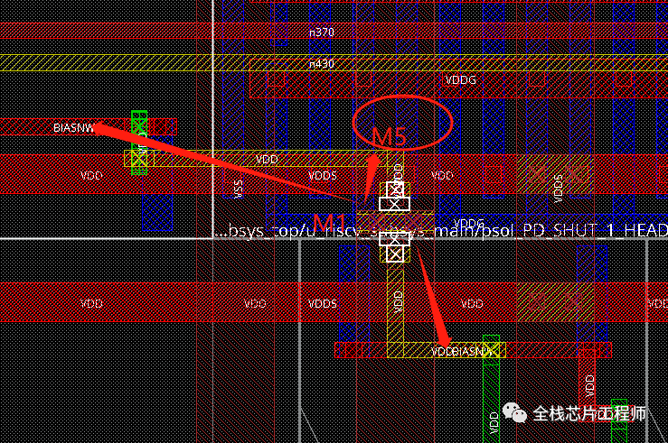
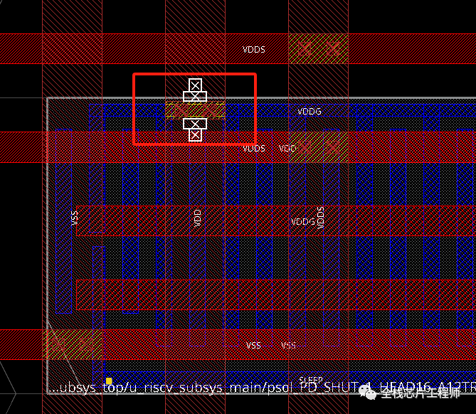
In the 7-day sprint PR training camp, some students asked why the second PG pin (VDDG) of the power switch cell is connected from M1 instead of M2. What problems might this cause? How to solve it?
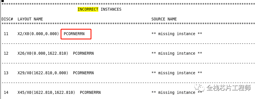
In the 7-day sprint PR training camp, some students asked how to handle LVS issues encountered by Jingxin SoC training camp students?
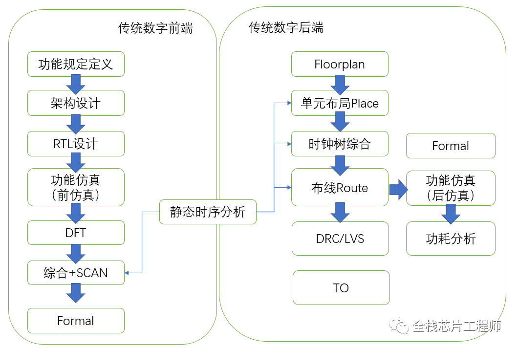
After completing the front-end design simulation and DFT of Jingxin SoC training, we come to the backend flow. This tutorial teaches you how to complete the digital backend flow with one click.
The script command to generate is as follows:
tclsh ./SCRIPTS/gen_flow.tcl -m flat all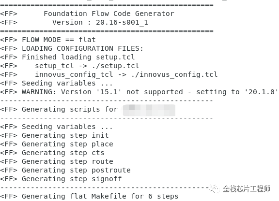
Before generating the flow script, you need to configure setup.tcl and other related parameters. For specific details, refer to the [the only one online] [full stack chip engineer] who provides self-developed Jingxin SoC front-end engineering, DFT engineering, and backend engineering, taking you through the entire process of SoC project design from algorithms, front-end, DFT to backend.
Students in the Jingxin SoC training camp asked why innovus reports an error when reading the completed floorplan def file? First, check the log:

Reading floorplan file – ./data_in/DIGITAL_TOP.def (mem = 1595.0M).
#% Begin Load floorplan data … (date=10/23 22:38:01, mem=1579.3M)
**ERROR: (IMPFP-710): File version unknown is too old.
In the past EDI era, we could load the floorplan by defining fp_file:
set vars(fp_file) "./data_in/DIGITAL_TOP.def"But now innovus has upgraded and abandoned the way of loading fp_file; of course, you can also use the old version of EDI9.1 and earlier to add fp_file and then save it as a new version, but this method is obviously unnecessary. Just as the log prompt says, checking the log is a very good engineering habit.
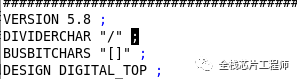
Input floorplan file is too old and is not supported in EDI 10.1 and newer.
You can use EDI 9.1 and before to read it in, then save again to create a new version.
The editor’s intuition tells me to check which def version the student saved?
The student’s save method is as follows:
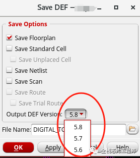
So how to solve it? Please join the Jingxin training camp for practice.
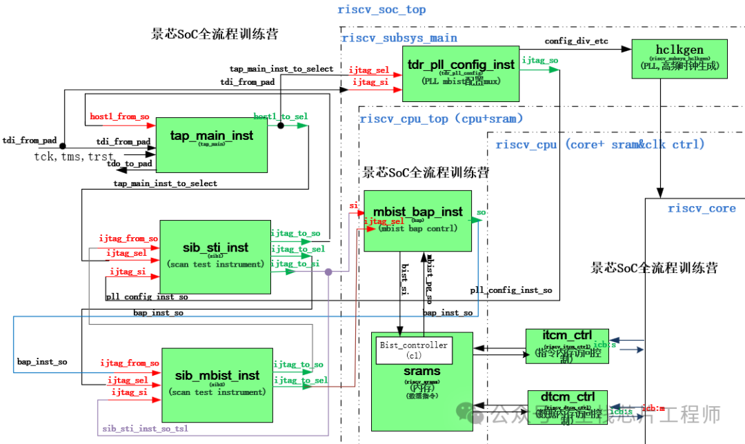
The Jingxin SoC uses many asynchronous FIFOs. Students interested in asynchronous RTL implementation can capture the asynchronous FIFO to check the layout connections:
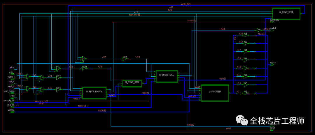
Check the area of all asynchronous FIFO cells;
dbget [dbget top.insts.pstatus unplaced -p].areaCheck the names of all asynchronous FIFO cells:
dbget [dbget top.insts.pstatus unplaced -p].nameSo how to extract asynchronous paths to observe the layout routing? How to report timing? For more content, refer to the knowledge star and SoC training camp.
Chip Full Process Training
Chip Training is about to increase in price, sign up contact the editor WeChat: 13541390811
-
Jingxin SoC front-end, mid-end, and backend low power full process practical training(price is less than 1/6 of peers)
-
Jingxin SoC front-end video + documentation + practical + one-on-one lifetime guidance practical training
-
Jingxin SoC mid-end video + documentation + practical + one-on-one lifetime guidance practical training
-
Jingxin SoC backend video + documentation + practical + one-on-one lifetime guidance practical training
-
12nm 2.5GHz A72 low power DVFS practical training(price is less than 1/3 of peers)
-
12nm 2.5GHz A72 DFT practical training(price is less than 1/3 of peers)
-
RISC-V MCU 40nm full chip PR practical training
-
DDR4/3 project practical training
-
MIPI CSI2 + ISP image processing + H.265 + USB + MAC practical training
-
Advanced Codec H.265/H.264 practical training
Chip Design Service introduction:
-
Providing SoC, MCU, ISP, CIS and other chip design, verification,DFT design services
-
Providing DDR/PCIE/MIPI/CAN/USB/ETH/QSPI/UART/I2C IP design
-
Providing backend design for 7nm, 12nm, 28nm, 40nm, 55nm, 65nm, 90nm
-
Providing customized chip design services and design training for universities and enterprises
In addition, the editor shares chip design, verification, DFT, and backend full process knowledge and a large number of technical documents in the knowledge star. Everyone is welcome to join the discussion and learning, and make progress together!

【Let every student design a SoC/MCU chip】
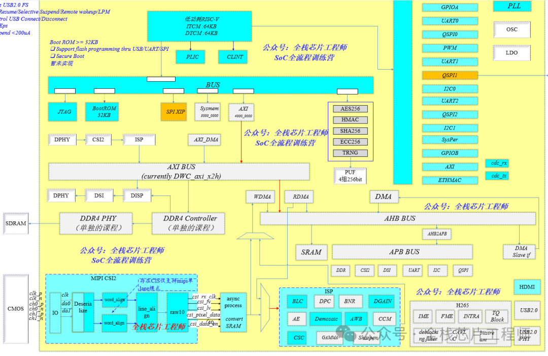
【The only one online】 Jingxin SoC is a low power ISP image processing SoC used for 【chip full process design training】, adopting a low power RISC-V processor, built-in ITCM SRAM, DTCM SRAM, integrating IPs including MIPI, ISP, USB, QSPI, UART, I2C, GPIO, Ethernet MAC controller, etc., designed using SMIC40 process.
-
High-speed interface Verilog design implementation -
From image algorithm to RTL design implementation -
MIPI, ISP’s Verilog implementation and simulation -
Lint, CDC checks and UVM verification -
Post-simulation
Just the content of the front-end course is equivalent to 5-6 courses from other training institutions.
-
DFT design (chip level) -
Synthesis logic synthesis (chip level) -
Low power UPF design, CLP technology -
Formal verification and other technologies
(3) In the SoC backend course, you will learn
-
Low power design
-
Layout and routing (low power FF flow) -
StarRC/QRC -
STA/Tempus -
Power analysis -
DRC/LVS design
Just the content of the backend course is equivalent to 3-4 courses from other training institutions.
Join the knowledge star and become part of the chip design knowledge treasure!
SoC training camp’s knowledge star