Since the introduction of the Cortex-A72 with out-of-order triple issue in February 2015, ARM launched the Cortex-A73 core in May this year, claiming that this core achieves the same or even better performance than the Cortex-A72 in its out-of-order dual-issue design. Is the Cortex-A73 really that impressive?
As a product numbered higher than the Cortex-72 and belonging to the Cortex-A7X series, why did A73 opt for a dual-issue design? The reasons are quite interesting. Firstly, although the Cortex-A73 and Cortex-A72 have a numbering difference of only 1, they come from two different design teams. The high-performance processor cores in the Cortex-A series are designed by two teams: the Texas team in Austin, USA is responsible for the highest performance IPs like Cortex-A15, Cortex-A57, and Cortex-A72, while the Cortex-A12, Cortex-A17, and Cortex-A73 are from the European design team of ARM. Secondly, from a product roadmap perspective, the goals pursued by ARM’s European design team are distinctly different from those of the Texas team; the European team is no longer pursuing extreme performance but rather a good balance between performance, power consumption, and area.
In ARM’s presentations, it can be seen that the power performance of the Cortex-A73 has further improved (indicating an increase in performance per watt), while the IPC remains basically on par with the Cortex-A72. It achieves performance exceeding that of Cortex-A73 by implementing a higher clock frequency. ARM’s official data shows that comparing the Cortex-A73 on a 10nm process with the Cortex-A72 on a 16nm process, the Cortex-A73 can reach a maximum frequency of 2.8GHz, with a performance increase of 30% and energy efficiency improvement of 30%.
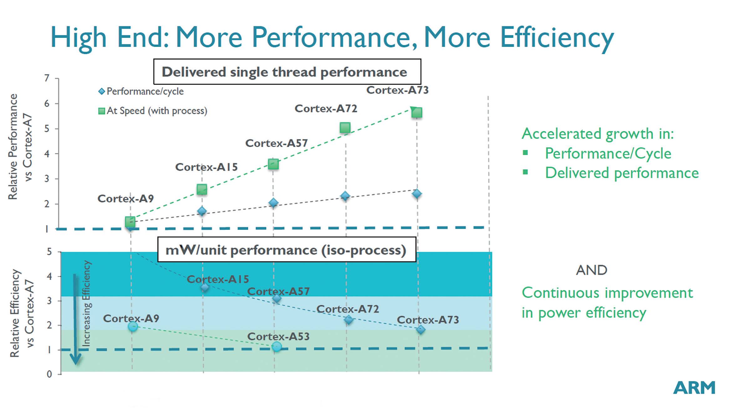
▲Performance and Power Comparison in ARM’s Presentation
Some may question, isn’t dual-issue inherently inferior to triple or quadruple issue?
“Multiple-issue” refers to the ability of a processor to execute two or more instructions in a single clock cycle. “Out-of-order” is short for out-of-order execution, meaning the processor can dynamically schedule instructions, executing those that must be executed later but have no actual execution conflicts earlier. These two structural design techniques require very complex and precise control and scheduling of the entire execution flow, thus out-of-order multiple issue is considered the cornerstone of modern high-performance processor microarchitecture.
Although dual-issue does indeed have an inherent limitation in issue width compared to triple or quadruple issue, the final performance is not necessarily so. Issue width is just one of many important design metrics in microarchitecture; there are many other significant metrics, such as:
1. The speed of branch prediction. Generally, it requires very few cycles to determine if a branch instruction will jump; the slower the branch prediction judgment speed, the more potential bubbles in the instruction fetch pipeline.
2. The accuracy of branch prediction. The accuracy directly affects whether the fetched instructions are correct; if not, it leads to pipeline flushes, wasting power and reducing performance.
3. Instruction cache hit rate and throughput. Even if the branch predictor quickly and accurately points to the instruction fetch address, if the instruction cache cannot supply the instructions quickly, performance will also suffer.
4. The number of read/write ports and shared arbitration in the register file. A register file that provides multi-port parallel read/write capability is one of the core components of an out-of-order wide-issue engine. However, multi-port register files take up a lot of area, and in practical designs, shared read/write ports are often used to reduce the number of required ports, making read/write port arbitration an important performance design element.
5. The design of the issue queue (reservation station). The issue queue is also a core component of the out-of-order multiple-issue engine; its design has many quantifiable performance metrics, such as the number of entries (depth), structure (multiple centralized issue queues or shared issue queues), and also difficult-to-quantify metrics, such as the data bypass network between the issue queue and other components.
6. Memory access reordering and address analysis capabilities. From a performance perspective, memory access (including the cache and memory subsystems) is a very important issue. Nowadays, designs typically also perform out-of-order execution for memory access instructions, but according to memory model regulations, out-of-order memory access must conduct address disambiguation analysis to ensure correct execution results. Aggressive disambiguation prediction can exchange a small number of correctable memory model violations for significant performance gains.
Thus, it can be seen that issue width only roughly measures a part of core performance; therefore, in the market, we often see examples where the same issue width has a significant performance gap, such as the out-of-order dual-issue Cortex-A73 and the out-of-order dual-issue Cortex-A9. Similarly, there are also cases where a lower issue width can achieve similar IPC to a higher issue width, such as the out-of-order dual-issue Cortex-A17 compared to the out-of-order triple-issue Cortex-A15, and the Cortex-A73 compared to the Cortex-A72.
So how is this achieved? Next, we will compare and analyze the core pipelines of Cortex-A73 and Cortex-A72.
The Cortex-A72 is an out-of-order triple-issue design, with an instruction fetch width of 128 bits (meaning 4 ARMv8-A instructions) per cycle and a decode width of 3 instructions per cycle. After decoding, ARMv8 instructions are broken down into smaller microinstructions (micro-ops or μops), with 5 microinstructions dispatched to 7 issue queues (IsQ) each cycle, indicating that Cortex-A72 has independent issue queue designs. Each of the two simple integer execution units is configured with an issue queue that can hold 8 microinstructions, as is the complex integer execution unit, and each of the two SIMD/floating-point execution units is configured with an issue queue that can hold 8 microinstructions, while the branch execution unit configured to handle branch instructions has an issue queue that can hold 10 microinstructions. Two address generation units (AGUs) are responsible for generating load and store addresses and share an issue queue that can hold 16 microinstructions. The pipeline length for simple integer operations is about 15 stages.
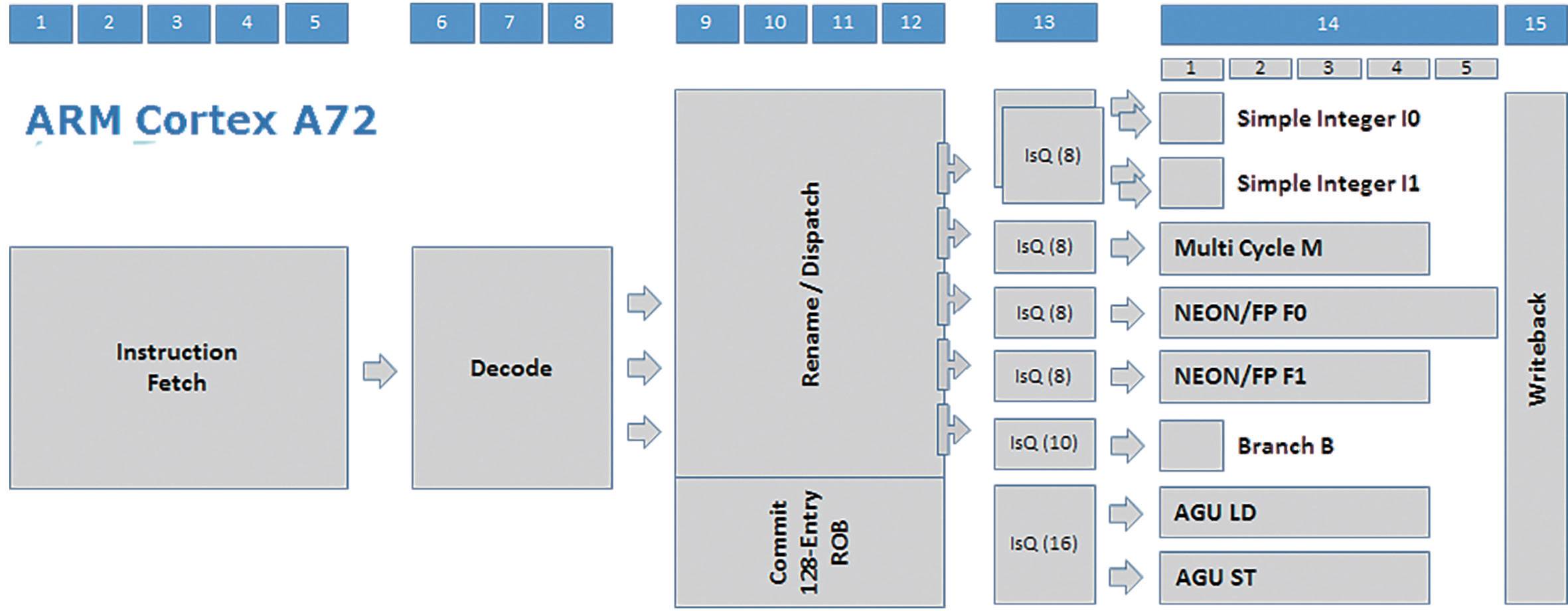
▲Cortex-A72 Core Pipeline
The Cortex-A73 has made several simplifications compared to the Cortex-A72. Firstly, the number of cycles required for instruction fetching has been adjusted from 5 cycles to 4 cycles, and the decode width has been reduced from 3 instructions to 2 instructions, but the number of cycles required has also been reduced from 3 cycles to 1 cycle, with a dispatch width adjusted to 4+2=6 microinstructions, where general integer instructions enjoy a dispatch width of 4 microinstructions (as shown in the upper half of the Cortex-A73 core pipeline diagram). SIMD and floating-point instructions, after an additional decoding cycle, will go through a separate dispatch channel of 2 microinstructions width (as shown in the lower half of the Cortex-A73 core pipeline diagram), presented to an issue queue shared by two SIMD/floating-point execution units. The dispatch logic can dispatch up to two microinstructions to any issue queue per cycle.
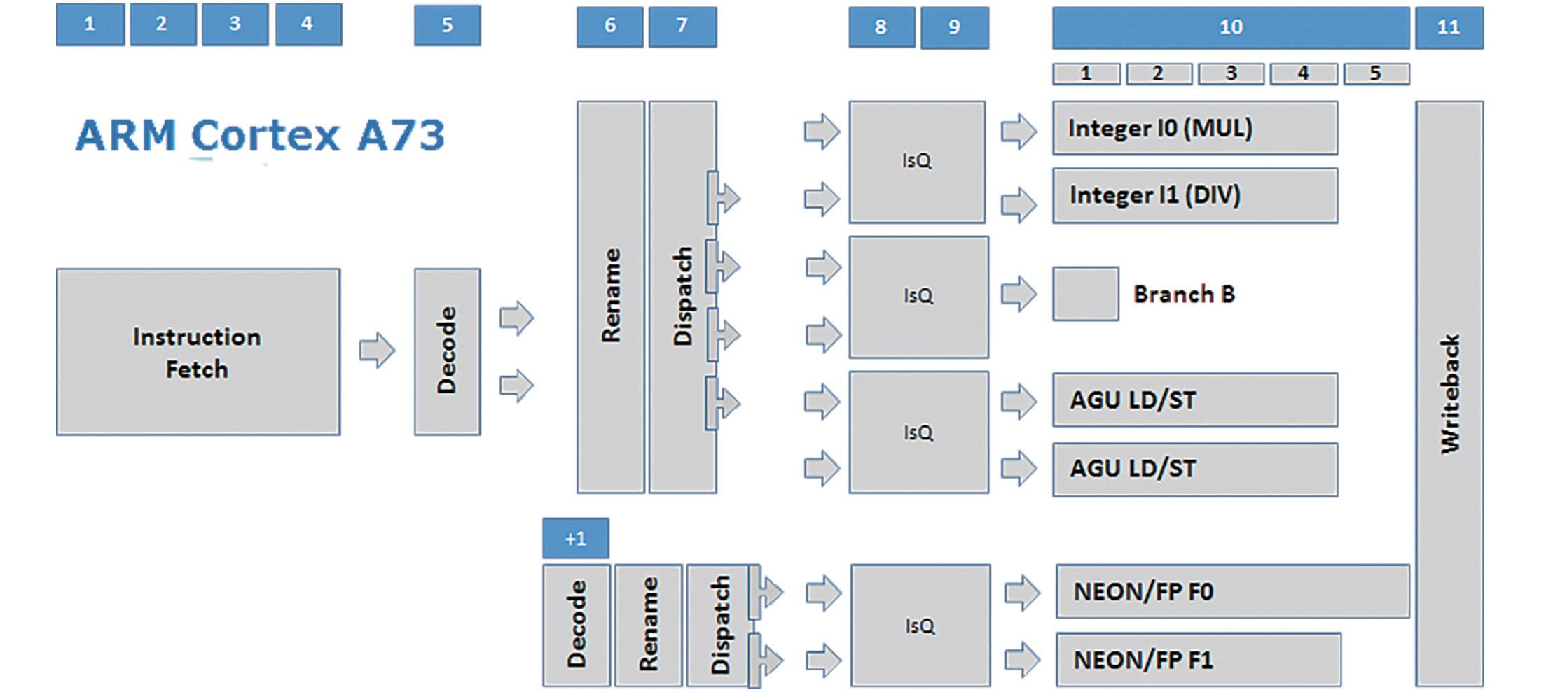 ▲Cortex-A73 Core Pipeline
The integer execution unit cluster has also been adjusted, primarily manifested as:
1. Generalization of Execution Units. For example, in the Cortex-A72, the simple integer execution unit and the complex integer execution unit are independent, but in the Cortex-A73, they are integrated, allowing both integer execution units in Cortex-A73 to execute both simple and complex integer operations, with one capable of performing integer multiplication and the other integer division. Additionally, the address generation units in Cortex-A73 no longer distinguish between loading and storing; both address generation units can perform both loading and storing.
2. Sharing of Issue Queues. The issue queues in Cortex-A73 are mostly shared between two execution units, for example, the two integer execution units share one issue queue, the two address generation units share one issue queue, and the two SIMD/floating-point execution units share one issue queue. In contrast, the more independent issue queue design of Cortex-A72 helps improve capacity utilization but may lead to performance degradation if the issue queue capacity is insufficient.
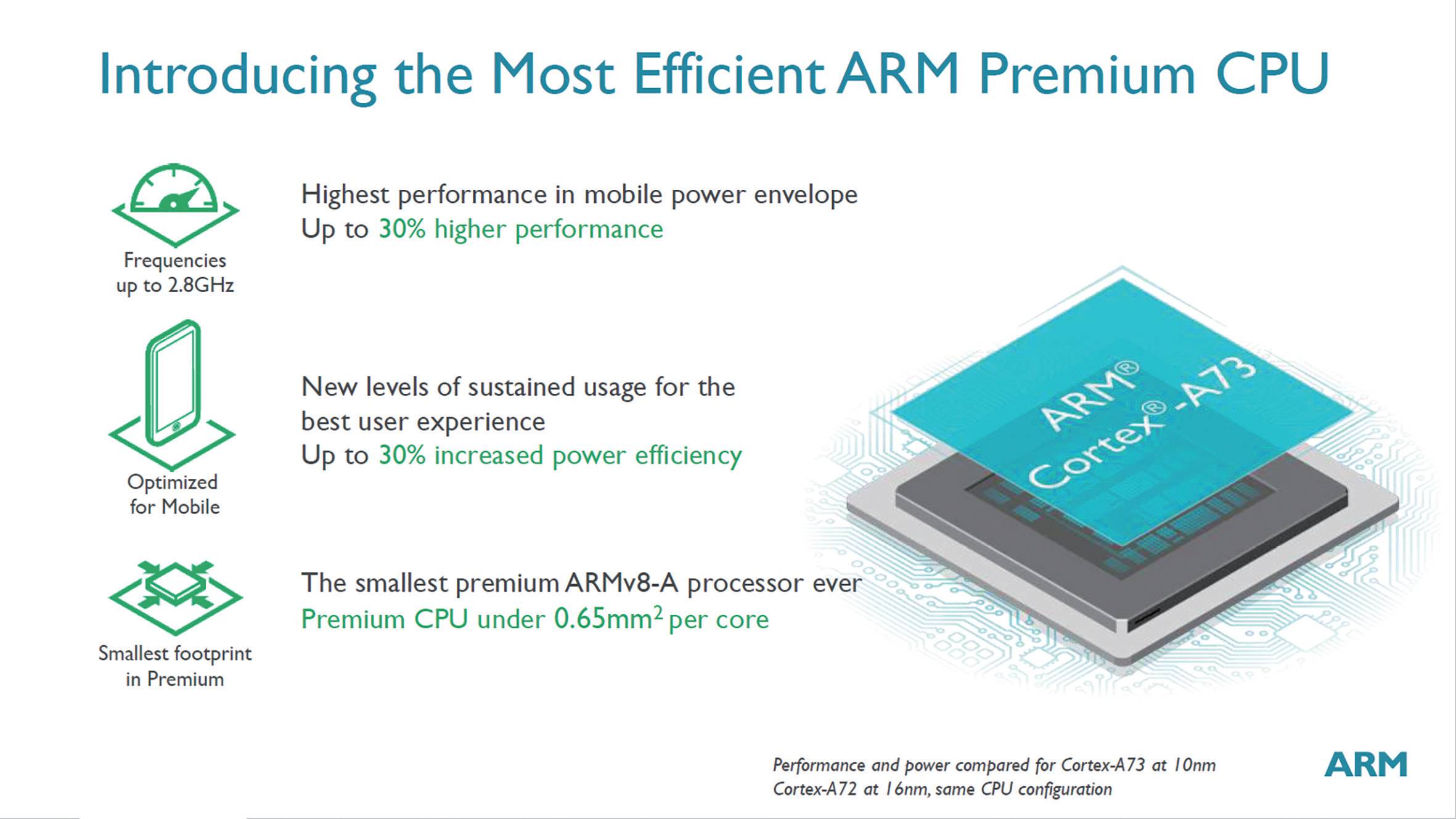
▲Official Comparison Data Presented by ARM
Based on the shortest execution cycle for branch instructions shown in the “Cortex-A73 Core Pipeline” diagram, the pipeline depth of the Cortex-A73 has also been reduced to 11-12 stages. Furthermore, ARM’s default L1 instruction cache size has been increasing; the default L1 instruction cache size for Cortex-A15 was 32KB, for Cortex-A57 and Cortex-A72 it was changed to 48KB, and for Cortex-A73 it has changed to 64KB, using 4-way set associative and a 64-byte cache line size.
In previous designs, even if the instruction fetch front end correctly predicted the instruction stream direction and the instruction cache provided data at maximum throughput, there were still pipeline bubbles during the breakdown of instructions into microinstructions. ARM claims that the Cortex-A73 core introduces the ability to detect whether such bubbles occur in advance and decodes microinstructions ahead of time to avoid bubble generation. It is speculated that this may involve a design similar to a uops cache.
In branch prediction, the Cortex-A73 uses a more advanced branch predictor, with a larger branch target address cache (BTAC), which is typically used to speed up the judgment speed of branch predictions. Generally, the larger the various table structures used by the branch predictor, the more branch history information can be retained, leading to less interference in branch instruction predictions and thus higher prediction accuracy and IPC. However, if the table structure is made too large, the time required to access the record table will also increase, thereby extending the decision time for branch prediction, which can be detrimental to performance.
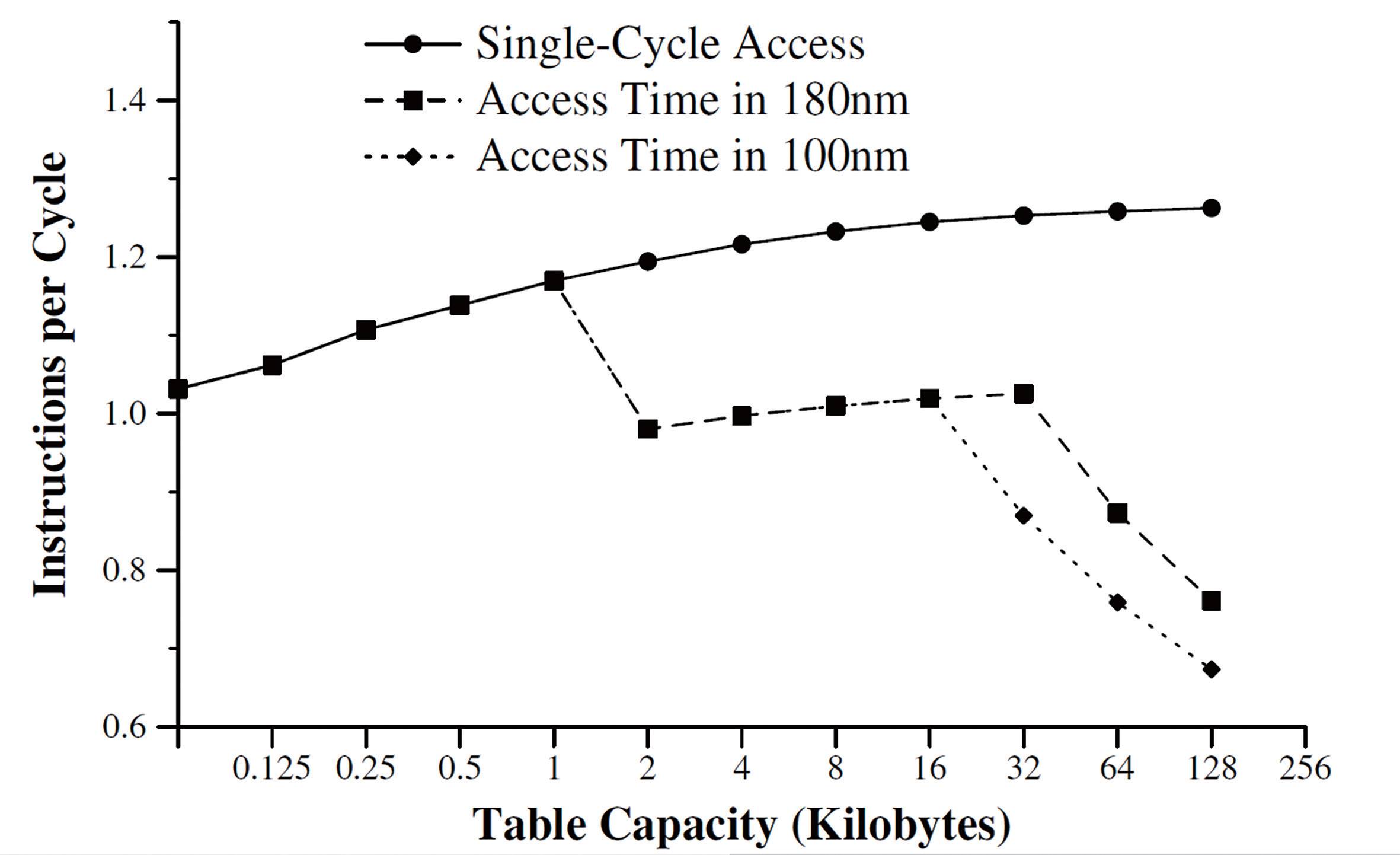
▲Relationship Between the Size of Branch History Record Tables and IPC at 180nm and 100nm Processes
To simultaneously improve the size of the record table required for branch prediction while shortening access latency, thereby controlling the time required for branch prediction, modern processor microarchitectures typically use multi-level record tables similar to multi-level caches. Usually, the first-level record table has a small capacity but is very fast, storing the most frequently used records, while the subsequent level record tables are larger, storing as many records as possible. The Cortex-A73 also employs a similar design approach, with a multi-level design for its branch target address buffer, where the first level can only store 64 branch target address records. Compared to the Cortex-A17, the Cortex-A73 introduces a new indirect branch predictor, reportedly consisting of a 2-way set associative structure with 256 entries, but without other related information, it is unclear how this indirect branch predictor differs from the design in Cortex-A72.
All branch predictors rely on storing historical records of branch instructions for prediction. For instance, when a branch instruction jumps or does not jump, this information is recorded in the branch history record table. If continuous jumps or non-jumps occur, it can be inferred that this branch has a significant bias, and the branch predictor will make predictions based on this. However, the number of dynamic branch instructions encountered during program execution is astronomical, and due to physical limitations, the branch history record table cannot be infinite, leading to many branch instructions sharing a single entry in the branch history record table, resulting in interference and inaccurate predictions.
In terms of register renaming methods, ARM claims to have made a “philosophical change in out-of-order execution methods,” which refers to the use of a register renaming method based on a physical register file. The advantage of the physical register file is that only one copy of each data needs to be retained throughout the out-of-order execution engine, and moving data only requires moving the pointer of the physical register file, significantly reducing the power overhead of moving data.
In summary, the streamlined and enhanced Cortex-A73 core can achieve a 25% reduction in core area under the same process, reaching a core area level similar to that of Cortex-A53.
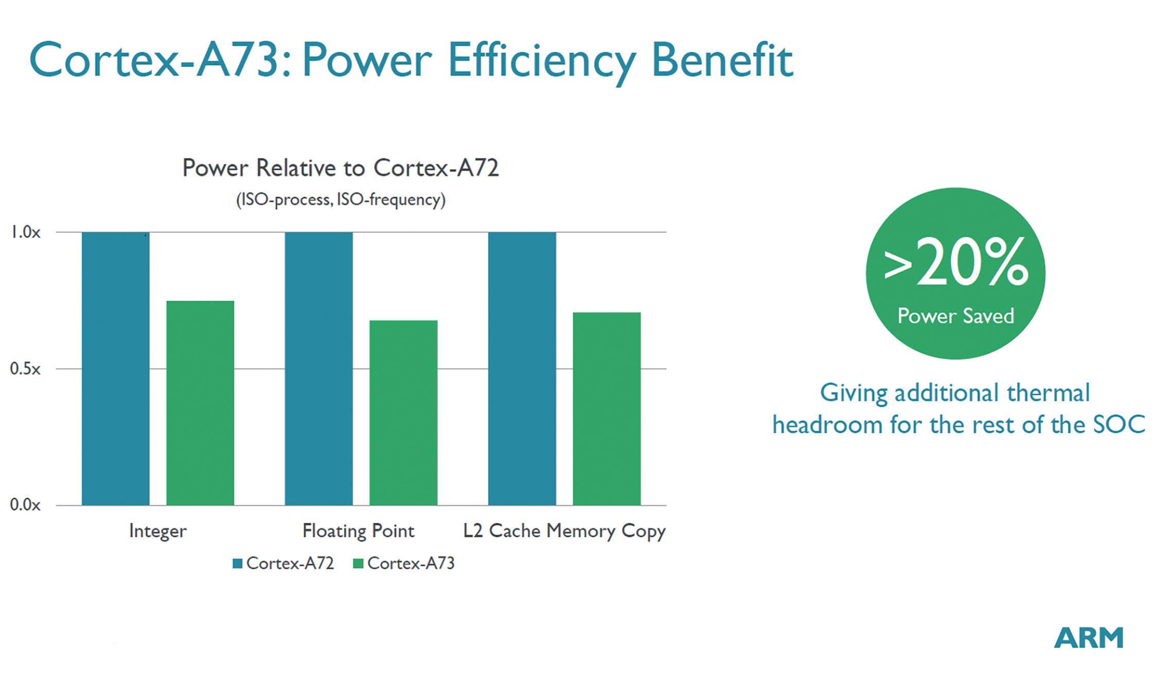
▲Core Area Comparison
The changes in the memory subsystem begin with the load/store buffer. ARM claims that the Cortex-A73’s load/store buffer can dynamically detect instruction issuance patterns and dynamically change the instruction issuance strategy upon certain specific events. For example, when stream memory access is detected, store operations will be issued at the fastest rate, which may facilitate the execution backend in the first-level cache or further down in the second-level cache or coherence unit to perform write merging and reduce bandwidth requirements.
Regarding the TLB, ARM has added a prefetcher for the main TLB of Cortex-A73 to handle stream memory access, ensuring that when stream memory accesses cross page boundaries, the main TLB is ready with new TLB entries, preventing TLB misses in such scenarios. The Cortex-A73’s TLB now supports two concurrent Table Walks and provides non-blocking access capabilities, allowing it to continue accepting other requests and output TLB hits during Table Walks.
Modern computer systems typically use virtual memory. The translation of virtual memory to physical memory addresses is done through page tables, which are generally maintained in memory by the operating system. In theory, every access to the cache requires the intervention of the page table for address translation; if every access needed to fetch the page table from memory, it would be too slow, hence TLB was born. TLB is essentially a cache for page table translations within the processor, allowing the processor to know the physical addresses corresponding to some commonly used virtual addresses without needing to access memory, significantly speeding up translation.
In the L1 cache, ARM has finally transitioned from a physical index + physical tag (PIPT) design to a virtual index + physical tag (VIPT), which can simultaneously ensure the reliability of physical index + physical tag and the performance of virtual index + virtual tag. This design takes advantage of the overlapping characteristics between page offsets and page number encoding with cache address indexing, using physical addresses as comparison tags within the cache, but accessing the cache using virtual addresses to avoid TLB latency. After completing the access to the cache’s tag array and outputting a complete set of cache address tags, the TLB’s virtual-to-physical address translation is also completed in parallel, allowing for quick determination of cache hits without generating memory address aliasing.
The Cortex-A73 features independent prefetchers for both L1 and L2 caches, supporting larger prefetch strides than ARM’s previous designs. ARM claims this prefetcher can help the Cortex-A73 achieve bandwidth close to theoretical maximum under stream memory access. The maximum configurable size of the Cortex-A73’s L2 cache is 8MB, double that of the Cortex-A72, and the L2 cache employs an inclusive design, simplifying cache coherence handling in multi-core processors but also leading to issues with cache data duplication, meaning the L2 cache always contains data from the upper L1 cache, wasting cache space. In the case of a strictly inclusive design, it may also lead to interference among multiple cores, resulting in performance loss.
▲Performance Comparison Between Cortex-A73 and Cortex-A72 at the Same Process and Frequency
Although the Cortex-A73 has downgraded from triple-issue to dual-issue, by strengthening other aspects, ARM claims its SPEC performance will be similar to that of the Cortex-A72, while improving near 10% in same-frequency performance on BBench, a 5% increase in NEON SIMD performance tested with the FFMPEG encoder (with more improvements expected in the next generation), and a 15% improvement in memory performance tested with the JMC stream copy in 64-bit mode, while power consumption decreases by 20%.
It is worth mentioning that the hardware power state management first introduced in Cortex-A35 also appears in the Cortex-A73. If ARM’s implementation of hardware power state management in the Cortex-A73 is successful, its dynamic power consumption could further decrease.
ARM claims that SoCs using the Cortex-A73 as the main core will hit the market by the end of this year. If this core can indeed achieve the numbers published in the ARM PPT, it will put greater pressure on other manufacturers developing their own cores through instruction set licensing. Whether the Cortex-A73, which has reduced issue width, can carry the flag from the Cortex-A72 remains to be seen.
The official WeChat group for MC’s benefits experience is now officially online. Various red packets will be sent in the group from time to time, various trial activities will be held, and various unexpected gifts will be given out. Interested in joining the group? Please add WeChat ID microcomputer2 as a friend, and the group owner will bring you into the group as soon as possible! We look forward to your joining!