This article highlights:
- Features and design points of the RK3588 DDR controller
- Power design differences for LPDDR4/LPDDR4X/LPDDR5
- 8/10 layer stack-up solutions and impedance control
- Practical layout and routing techniques and timing requirements
- Common design pitfalls and avoidance guide
1. Introduction to RK3588 DDR Controller
The RK3588 DDR controller supports LPDDR4/LPDDR4X/LPDDR5 standards, featuring:
- 64-bit data bus, 4 x 16-bit channels, supporting up to 32GB
- Dual-channel 32-bit configuration must use the same capacity chips
- Supports low power modes such as Power Down and Self Refresh
- Dynamic PVT compensation and programmable ODT impedance adjustment
Data signal pin distribution (Figure 1): shows the pin arrangement for CH0 channel 16-bit data signals (DQ0~DQ15), mask signals (DM0~DM1), and data strobe signals (DQS0~DQS1).
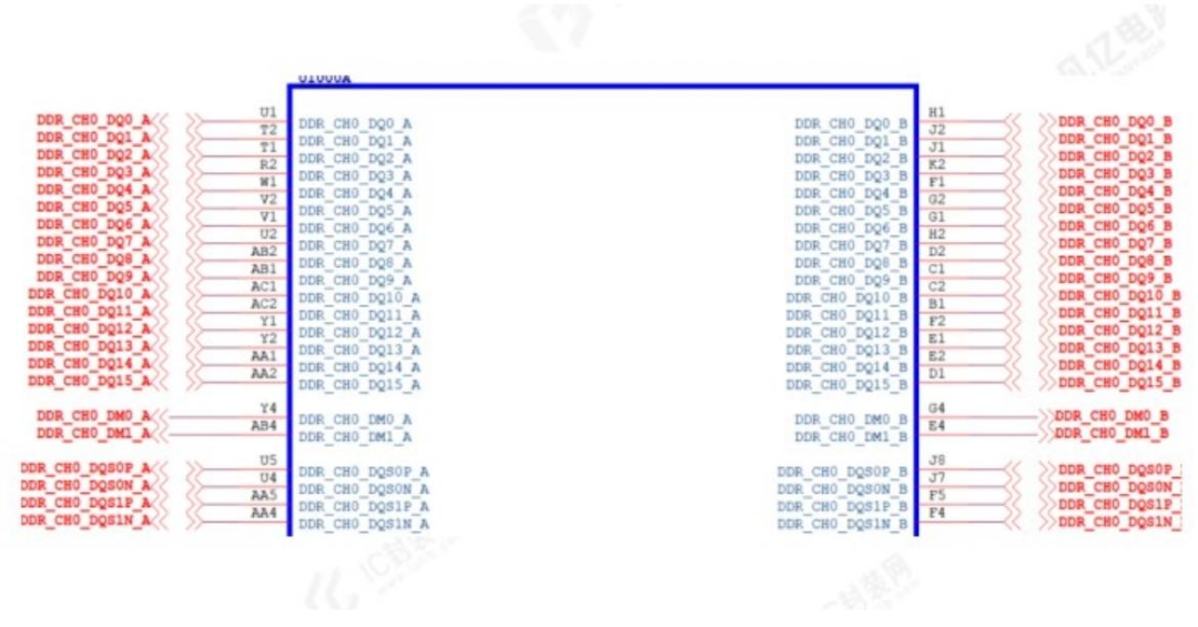
Figure 1 RK3588 DDR partial data signal pins
Address control signal pins (Figure 2): includes address lines (A0~A6), clock (CLK/CLKN), chip select (CS), reset (RESET), and other control signals.
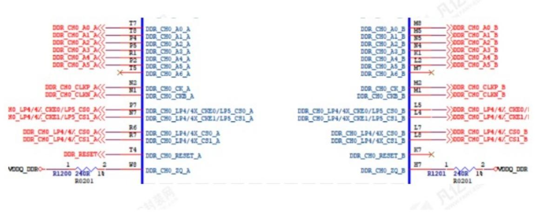
Figure 2 RK3588 DDR partial address and control signal pins
Power signal pins (Figure 3): different types of DDR require power rails such as VDDQ, VDD2, VDD1_1V8, etc.
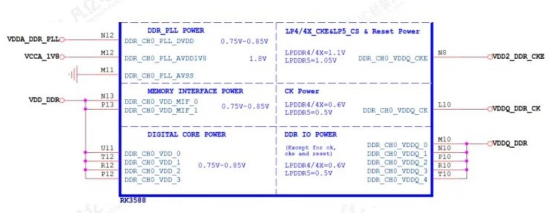
Figure 3 RK3588 DDR partial power pins
2. Power Design and Power-Up Timing
1. Power Voltage Requirements
RK3588 DDR PHY Power Supply (Table 1):
- VDDQ: LPDDR4/4X is 0.6V, LPDDR5 is 0.5V
- VDD2: LPDDR4/4X is 1.1V, LPDDR5 can switch between 0.9V/1.05V
- VDD1_1V8: fixed at 1.8V
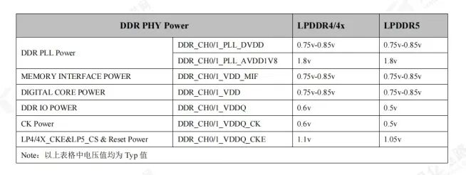 Table 1 RK3588 DDR PHY power supply
DDR Chip Power Supply (Table 2):
- VDDQ: LPDDR4 is 1.1V, LPDDR4X is 0.6V, LPDDR5 is 0.5V
- VDD2: LPDDR4/4X is 1.1V, LPDDR5 is 1.05V (can be as low as 0.9V)
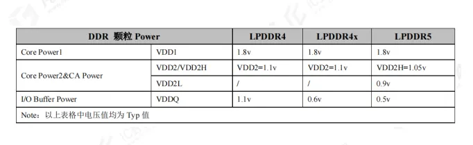
Table 2 LPDDR4/4X/LPDDR5 power supply
2. PMIC Configuration Solutions
Dual PMIC Solution (RK806-2):
- VDDQ adjustment circuit (Figure 4): sets output voltage through FB9 voltage divider resistors
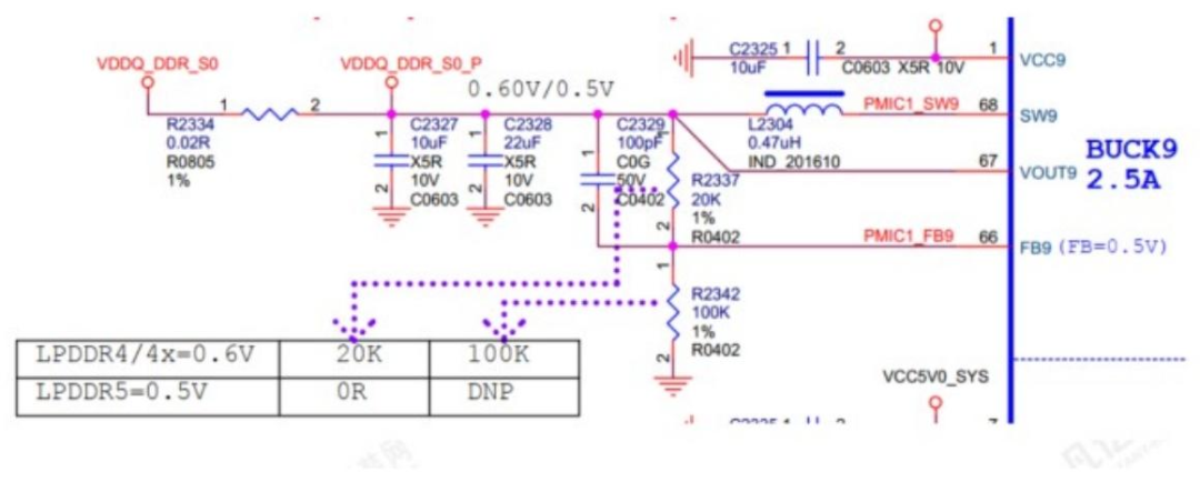 Figure 4 RK806-2 BUCK9 FB parameter adjustment
- VDD2 adjustment circuit (Figure 5): also set through FB9, LPDDR4/4X is 1.1V, LPDDR5 is 1.05V
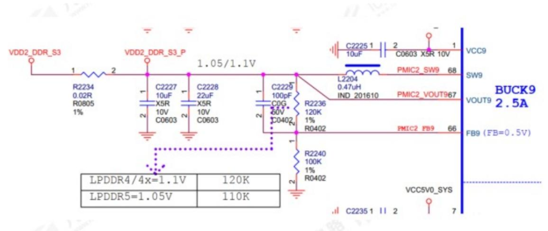 Figure 5 RK806-2 BUCK9 FB parameter adjustment
Single PMIC Solution (RK806-1):
- VDDQ adjustment (Figure 6)
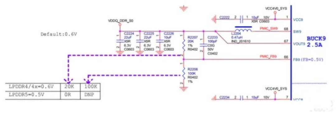 Figure 6 RK806-1 BUCK9 FB parameter adjustment
- VDD2 adjustment (Figure 7)
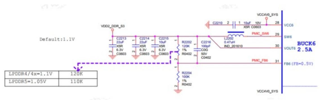 Figure 7 RK806-1 BUCK6 FB parameter adjustment
LPDDR4/LPDDR4X Compatible Design (Figure 8): selects corresponding power rails through different resistor configurations.
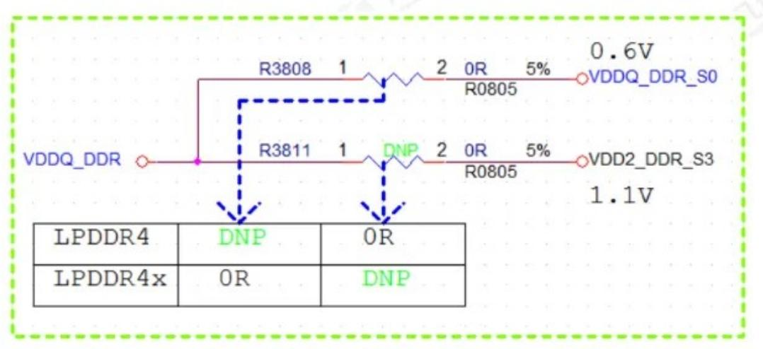
Figure 8 LPDDR4/LPDDR4X compatible design power selection
3. Power-Up Timing Key Points
- During self-refresh, DDR_CH_VDDQ_CKE must maintain power supply
- LPDDR5 supports DVFSC mode, using 1.05V for high frequency and 0.9V for low frequency
- LPDDR5 introduces WCK clock, with a frequency that can be 2 or 4 times that of CK
3. Stack-Up and Impedance Design
1. 8-Layer Through-Hole Board (1.6mm)
Stack Structure (Figure 9): TOP-Gnd-Signal-Power-Gnd-Signal-Gnd-Bottom
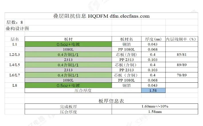
Figure 9 Recommended stack for 8-layer through-hole 1.6mm thickness
Impedance Line Width (Figure 10):
- Top layer 40Ω line width approximately 5.8mil
- Inner layer 40Ω line width approximately 6.8mil
- Differential 80~100Ω corresponding to different line widths / line spacing
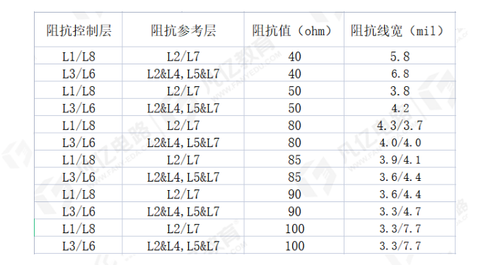 Figure 10 8-layer through-hole 1.6mm thickness various impedance line widths and spacings
2. 10-Layer HDI Board
1st Stage HDI (Figures 11/12):
- Stack: TOP-Signal/Gnd-Gnd/Power-Signal-…-Bottom
- Impedance control: 100Ω differential line width / spacing approximately 3.3/4.7mil
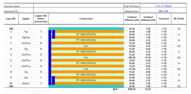 Figure 11 10-layer 1st stage HDI board stack design
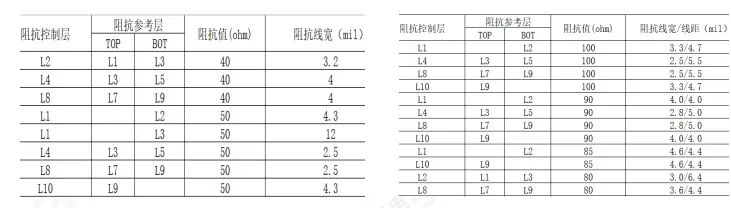
Figure 12 10-layer 1st stage HDI board impedance design
2nd Stage HDI (Figures 13~15):
- Single-ended impedance: 45Ω line width approximately 3.1mil, 50Ω approximately 2.6~4.2mil
- Differential impedance: 85~100Ω corresponding to different line widths / spacings
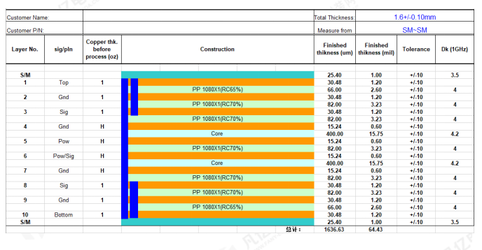 Figure 13 10-layer 2nd stage HDI board stack designFigure 14 10-layer 2nd stage HDI board single-ended impedance design
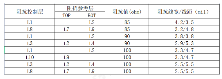
Figure 15 10-layer 2nd stage HDI board differential impedance design
4. Impedance Control Requirements
Various signal impedance standards:
- DQ, DM, address control signals: 40Ω±10% (Figures 16/17)
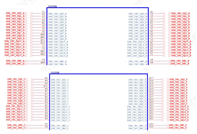
Figure 16 DQ, DM impedance lines for CH0 and CH1 channels
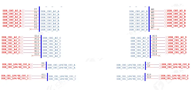
Figure 17 Address and control impedance lines for CH0 and CH1 channels
- CKE signal: 50Ω±10% (Figure 18)
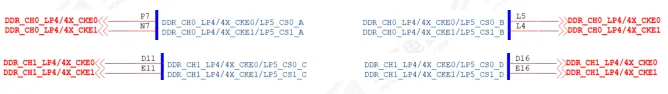
Figure 18 CKE impedance lines for CH0 and CH1 channels
- DQS, CLK differential signals: 80Ω (allowable 90Ω±10%) (Figure 19)
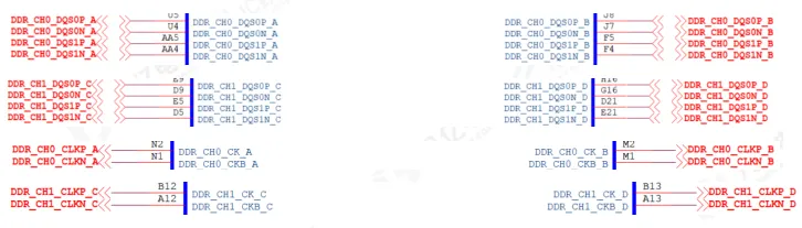
Figure 19 DQS and CLK differential impedance lines for CH0 and CH1 channels
5. Practical Guide to Layout and Routing
1. Prioritize Using Manufacturer Templates
Rockchip provides validated DDR layout templates, including:
- Relative positions of chips and memory
- Power filtering capacitor layout
- Copper pouring spacing requirements
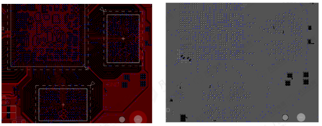
Layer 1 DDR circuit routing diagram Layer 2 DDR circuit routing diagram
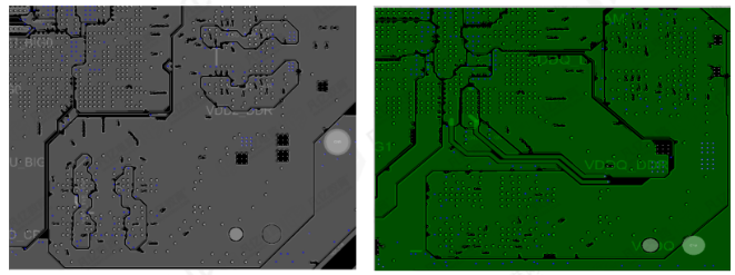
Layer 3 DDR circuit routing diagram Layer 4 DDR circuit routing diagram
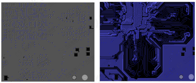
Layer 5 DDR circuit routing diagram Layer 6 DDR circuit routing diagram
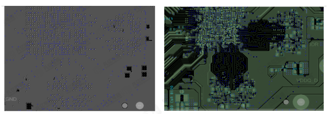
Layer 7 DDR circuit routing diagram Layer 8 DDR circuit routing diagram
2. Key Routing Techniques
Ground Via Design (Figure 20):
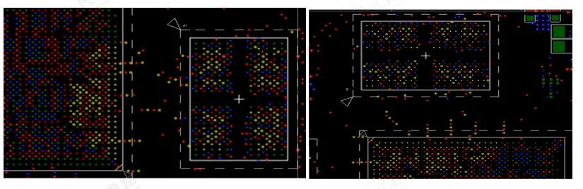
Figure 20 RK3588 ground via diagram
- Strictly configure GND vias according to the template
- Signal layer transitions require adding GND return vias (Figure 21)
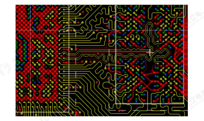
Figure 21 Signal layer transition adding ground via diagram
- Optimize via positions to avoid signal crosstalk (Figure 22)
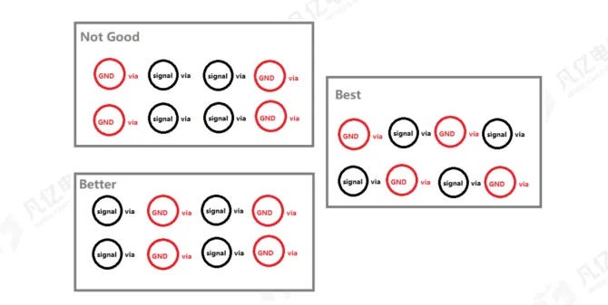
Figure 22 Return ground via position diagram
Reference Plane Integrity:
- Maintain GND plane integrity (Figure 23)
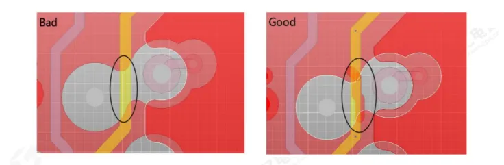
Figure 23 Ground plane segmentation completion diagram
- Serpentine routing should be avoided as much as possible, and if necessary, maintain spacing > 3W (Figure 24)
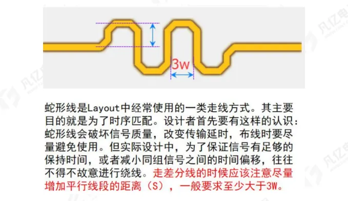
Figure 24 Serpentine routing diagram
- Consider via delay effects (Figure 25)
Figure 25 Via delay diagram
Power Via Configuration:
- VDD_DDR/VDDQ_DDR/VDD2_DDR: ≥6 0503 vias
- VDD1_1V8_DDR: ≥2 0402 vias
- Capacitor pads: 0603/0805 package recommends one pad with two vias
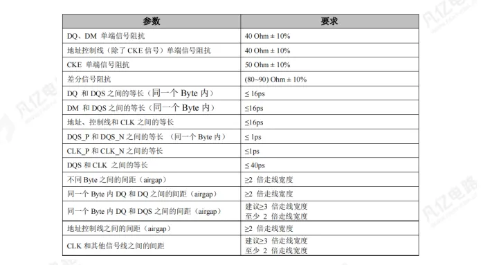
6. Timing Requirements
Equal Length Control:
- Within the same byte DQ-DQS, DM-DQS: ≤16ps
- Address/control and CLK: ≤16ps
- Differential pairs internally: ≤1ps
- DQS and CLK: ≤40ps
LPDDR4 impedance and timing table
Spacing Requirements:
- Between different bytes: ≥2 times line width
- Within the same byte DQ-DQ: ≥2 times line width (recommended > 3 times)
- CLK and other signals: ≥2 times line width
7. Common Design Pitfalls
- DQ/CA signal line swapping: not supported, must be confirmed with the manufacturer
- ZQ/ODT resistor configuration errors: ZQ must be 240Ω±1%, ODT_CA must be 10kΩ±5%
- Power plane segmentation: causes incomplete return paths
- Differential lines not equal length: affects signal synchronization
- Ignoring via delay: causes timing deviations
Conclusion
The RK3588 DDR circuit design is a systematic project, from power design to stack planning, from impedance control to timing optimization, every aspect is crucial. It is recommended to prioritize using Rockchip’s original templates, and if designing independently, be sure to perform simulation verification and confirm with FAE.
 Note:This article is an original piece by Fanyi Education, please indicate the source when reprinting!For submissions/recruitment/advertising/course cooperation/resource exchange, please add WeChat: 13237418207
Want to understand DC-DC converter SW signal testing? Please keep this practical methodology handy
2025-09-08
Is your electronic product durable? It all depends on whether the copper in the PCB is thick enough!
2025-09-04
Newbie-friendly! A tutorial on directly adding PCB packages in Mentor PADS is here
2025-09-04
Stacking principles in PCB design
2025-09-03
