Previously, we introduced how to make a logic analyzer and oscilloscope using RP2040. Today, we will build a logic analyzer using FPGA.
Currently, the mainstream architecture of logic analyzers in China uses FPGA + USB PHY. The combination of the advantages of FPGA and the high accessibility of USB has allowed it to occupy the mid-to-high-end market.
Today, we will use FPGA to build a logic analyzer. For universality, we choose serial communication for host communication, which greatly increases portability.
Overall Architecture
This project consists of 7 modules to implement the logic analyzer’s functionality: trigger controller, sampling rate counter, buffer, control module, and UART communication.
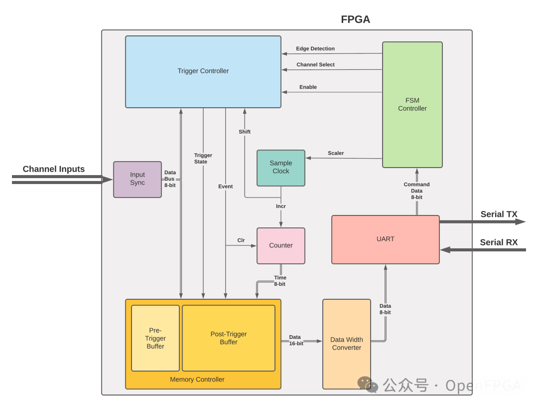
Trigger Controller
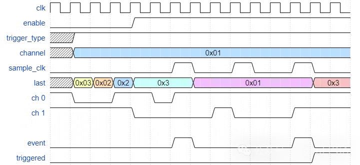
This module allows users to configure trigger conditions on the channels. The condition can be set via the GUI to be either a falling edge or a rising edge. The sampling rate signal is used to inform the trigger controller when new input data is available. If the new data does not match the current data, a signal will be sent to other modules. Once the trigger condition matches, a trigger status signal will be sent to the buffer.
Sampling Rate Counter
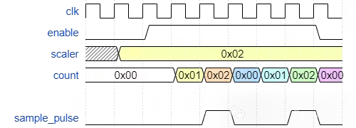
The system uses a 16-bit divisor to inform the logic analyzer what the sampling frequency should be. The sampling rate signal controls the frequency at which new data moves into the trigger controller and the frequency at which the timestamp counter should increment. In the GUI, this divisor needs to be combined with the FPGA clock frequency to obtain timing information from the relative timestamps.
Timestamp Counter
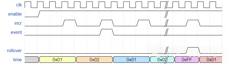
The system uses an 8-bit register to count the number of sampling clock pulses. This register is connected to the input data and then saved to the buffer. The timestamp counter increments on each sampling clock, tracking the relative time between events. If an event occurs, the counter resets to 1 and resumes counting. If the counter overflows, a signal is sent to the memory controller to start a new entry in the buffer. An enable signal is used to keep the counter at 1 until capturing begins.
Buffer
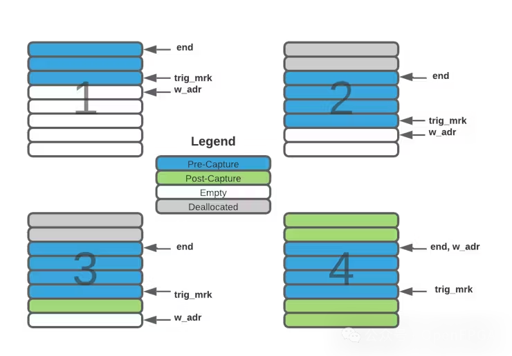
The buffer stores timestamps and data in RAM. New data begins to record in the buffer each time an event or timestamp flip signal is received. Before the trigger condition occurs, this module acts as a circular buffer, continuously overwriting previous entries. The size of this circular buffer can be programmed in the GUI, occupying a proportion of the entire buffer from 10% to 90%. Once the trigger condition occurs, the buffer acts as a FIFO, filling the remaining memory. Once full, the controller module receives a signal and reads the data line by line.
UART Communication
This module simply waits for the host PC to send bytes and forwards commands to the controller module.
Using the GUI
Main menu capture button
-
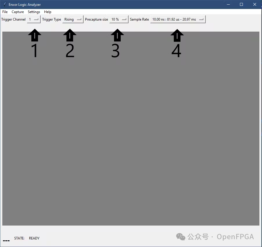
1: Select which channel to observe the trigger condition.
-
2: Set the trigger type to either rising edge or falling edge.
-
3: Set the data ratio before the trigger event.
-
4: Set the sampling rate, where the first number represents the sampling interval rate, and the next two numbers represent the minimum and maximum recording time, respectively.
-
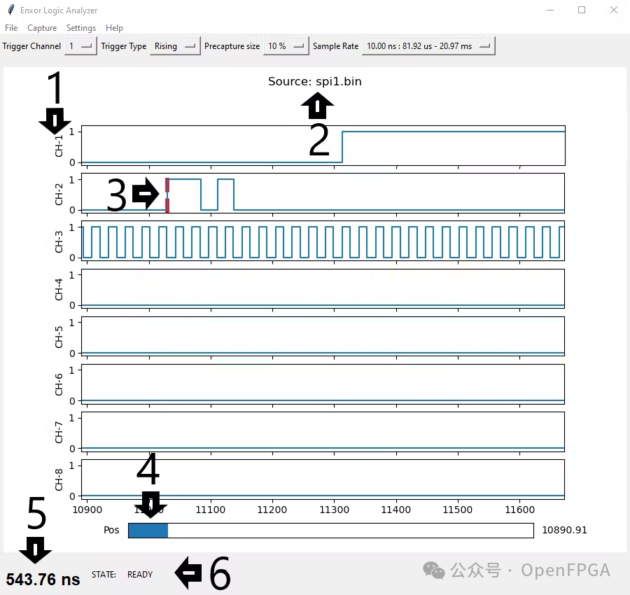
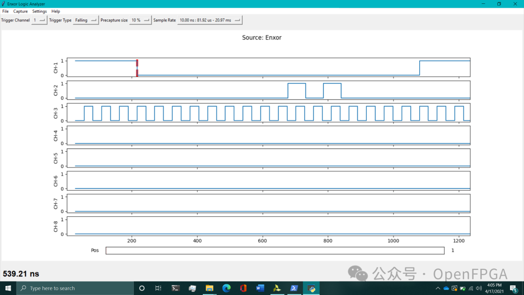
1: Channel name.
-
2: Indicates where the data comes from. If loaded from a file, set to the filename; if data comes directly from the logic analyzer, set to Enxor.
-
3: The red bar indicates the position where the trigger point occurs.
-
4: The position slider controls the x-axis. Click and drag the slider to move it to a new position.
-
5: Time interval measurement. Click on any point on the waveform and then click the second point to display the time between the two points.
-
6: Status of the logic analyzer. The READY state indicates that the logic analyzer is ready to start capturing. When the logic analyzer is enabled but not yet triggered, the state will be WAITING. After the trigger event, the state will be TRIGGERED. If capturing is stopped midway, the state will be STOPPED.
Screenshot during operation
Project Link
https://github.com/lekgolo167/enxor-logic-analyzer
Conclusion
This project is suitable for those who want to learn and study the architecture of logic analyzers. If you want to understand the USB PHY architecture of logic analyzers, feel free to leave a message, and we will update it as soon as possible~