

Click here to download the materials (3rd update)

Here are some resources for everyone, copy and reply with the following keyword to receive
Practical Power Supply Circuit


About Today’s Post
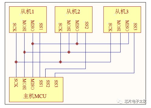
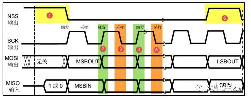
1. Start and stop signals of communication:
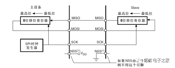
The NSS signal line transitions from high to low, which is the start signal for SPI communication.
The NSS signal transitions from low to high, which is the stop signal for SPI communication, indicating the end of the communication and cancelling the selection state of the slave.
2. Data Validity

-
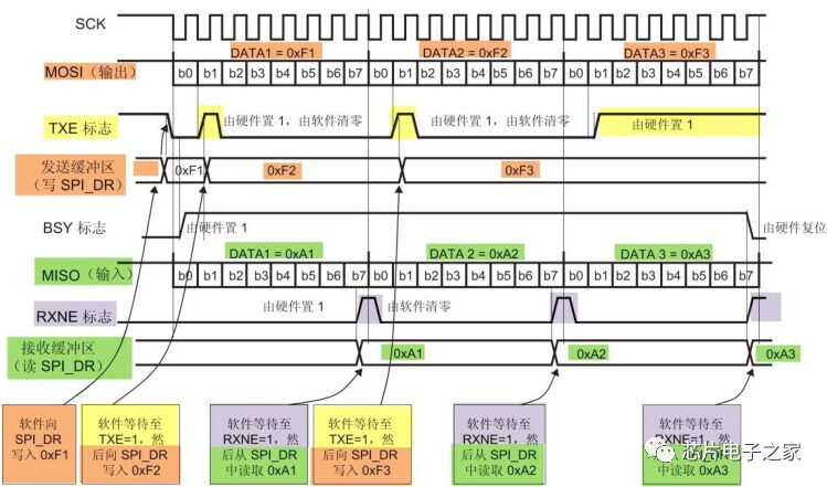
Control the NSS signal line to generate the start signal (not shown in the diagram);
-
Write the data to be sent into the “Data Register DR”; this data will be stored in the send buffer;
-
Communication begins, SCK clock starts running. MOSI sends the data from the send buffer bit by bit; MISO stores the data bit by bit into the receive buffer;
-
When a frame of data has been sent, the “TXE flag” in the “Status Register SR” is set to 1, indicating that a frame has been transmitted and the send buffer is empty; similarly, when a frame of data has been received, the “RXNE flag” is set to 1, indicating that a frame has been transmitted and the receive buffer is not empty;
-
Wait for the “TXE flag” to be 1; if more data needs to be sent, write data again to the “Data Register DR”; wait for the “RXNE flag” to be 1; the contents of the receive buffer can be obtained by reading the “Data Register DR”.
—Click below to search for keywords—
(Disclaimer: This article is compiled to disseminate relevant technical knowledge; some collected materials are copyrighted by their original authors)


Previous Selections
▲Multisim simulation example materials
▲Electronic circuit videos | Improve learning in analog and digital electronics
▲300 sets of electronic circuit analysis | Video animated tutorials
▲Switching power supply video repair tutorial | 164 episodes
▲Mini Program Development Technical Tutorial
▲Electronic circuit hardware design switching power supply analog and digital design video DIY hard tutorial
▲PCB design routing detail explanation (illustrated | highly recommended)
▲PCB && USB differential routing experience and lessons
▲0-ohm resistor usage finally summarized
▲PCB—The role of serpentine lines explained
▲Is it necessary to cover copper under power inductors?
▲Teach you how to design schematic diagrams
▲Introduction to the principles and applications of varistors, discharge tubes, voltage regulators, and TVS
▲The principles and differences of DC-DC and LDO
▲Question: Why does this circuit burn out the MOS tube?
▲The datasheet of components, it took a long time to understand how to read it
▲Some common tips for circuit board repair
▲MATLAB made confession tool with code
▲Introduction to the principles of lithium battery protection boards
▲Must-consider factors in LDO design
▲Usage of transistor and MOS driver circuits
▲How to consider analog ground and digital ground in circuit design
▲Power supply board layout considerations
▲100 knowledge points on PCB layout and routing | Including video
▲60 essential skills for circuit design
▲Detailed explanation of voltage followers
▲MOS applications, just discussing how to apply
▲Design of PIR infrared sensor amplification circuit
▲Deep learning in switching power supplies
▲Common circuits of voltage comparators
▲The 12th Freescale | Memories
▲C language | Unions, structures
▲Design of a thermal detection circuit
▲Some thoughts on switching power supply layout
▲STM32 drives 16-bit ADC
▲Disassembly of Huawei mobile phone power supply #Craft
▲Selection of power supply chips
▲Precise current direction analysis #MOS circuit
▲Starting and automatic shutdown of LDO
▲Analysis of large current starting from capacitance and inductance formulas
▲Microcontroller driving MOS circuit applications
▲Differences between transistors and MOS tubes in circuit design
▲How to make the 7805 output voltage reach 10V
▲Switching circuit to achieve the function of turning off the crystal oscillator
▲How to understand input and output capacitors in LDO
▲These two capacitors and resistors in switching power supplies
▲All buffering and absorption circuits in switching power supplies
▲Tips for using 10uF and 0.1uF capacitors in parallel