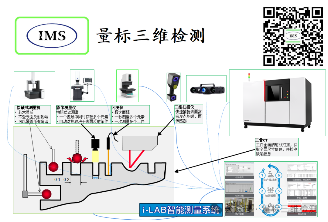
In today’s highly digitalized era, semiconductors are crucial components of electronic devices, making their quality and reliability essential. Industrial CT (Computed Tomography) technology, as an advanced non-destructive testing method, is gradually demonstrating its unique advantages and broad application prospects in the semiconductor field.
1. Introduction to Industrial CT Technology
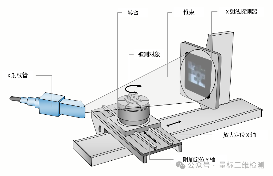
Industrial CT is a technology that uses X-rays to perform tomographic scans of objects and reconstructs three-dimensional images through computer processing. It provides detailed information about the internal structure of objects without causing damage, including defects, material distribution, and structural integrity.
2. Applications of Industrial CT in the Semiconductor Field
(1) Chip Packaging Inspection
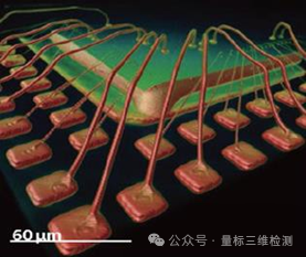
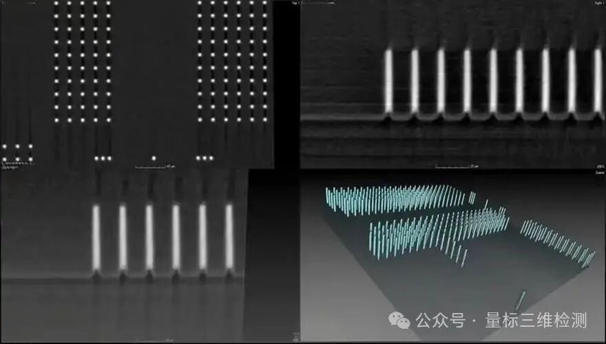
- Wire Bonding Inspection: Industrial CT can clearly display the shape, position, and connection status of wires, detecting issues such as wire breakage and cold solder joints.
- Packaging Material Inspection: It can detect defects such as bubbles, cracks, and delamination within the packaging materials, ensuring the reliability of the packaging.
(2) Wafer Inspection
- Wafer Defect Inspection: It can identify defects on the surface and inside the wafer, such as crystal defects, impurities, and cracks, improving wafer quality.
- Wafer Flatness Inspection: Accurately measures the flatness of the wafer, providing important data for subsequent processing.
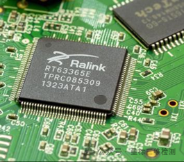
(3) Semiconductor Device Inspection
- Internal Structure Analysis: Industrial CT can reveal the internal structure of semiconductor devices, such as the electrode connections of transistors and the plate structure of capacitors, aiding in design and manufacturing optimization.
- Failure Analysis: When semiconductor devices fail, industrial CT can help determine the cause of the failure, such as whether there are short circuits, open circuits, or leakage issues.
3. Advantages of Industrial CT in the Semiconductor Field
(1) Non-destructive Testing
Industrial CT does not damage semiconductor products, allowing them to be reused or further processed after inspection, reducing resource waste.
(2) High Resolution
It can detect small defects and structural anomalies with resolutions reaching micrometers or even nanometers, meeting the semiconductor industry’s demand for high-precision inspection.
(3) Three-dimensional Visualization
Provides three-dimensional images, allowing inspectors to intuitively understand the internal structure of semiconductor products, facilitating the discovery of potential issues and analysis.
(4) Good Repeatability
The inspection results have high repeatability, unaffected by subjective factors from operators, ensuring accuracy and reliability in testing.
4. Outlook
The application of industrial CT technology in the semiconductor field provides strong support for improving the quality and reliability of semiconductor products. By inspecting chip packaging, wafers, and semiconductor devices, potential issues can be identified in a timely manner, manufacturing processes can be optimized, production costs can be reduced, and the development of the semiconductor industry can be promoted. With continuous technological advancements, the application of industrial CT in the semiconductor field will become more widespread and in-depth, making greater contributions to innovation and development in the semiconductor industry.
For more details, please contact:
Mr. Wang
13651735140
Interested friends can follow our public account to learn more about products and services.
Related Articles:
Industrial CT Inspection Services
Blue Light Scanning Inspection Services
Coordinate Measuring/Scanning/Industrial CT Accessories, Software, and Services
Getting Closer to Industrial CT–Structure and Applications
Non-destructive Perspective: Applications of Industrial CT Technology in Precision Casting Inspection
Getting Closer to Industrial CT–Three-dimensional Imaging Principles
How to Digitally Transform the Measurement Room–Digitalization of Measurement Rooms
Three-dimensional Measurement of Standards–AI Experts in the Measurement Field