In early 2024, based on project requirements, the read and write functionality of SATA hard drives was developed on the K7 board. At that time, considering future board upgrades, higher-speed PCIe NVMe M.2 hard drives could be used. Relevant information was researched: a project from Hanyang University was referenced for related design. This experiment is based on the aforementioned PCIe Gen3 X4 to implement read and write testing of NVMe hard drives.
FPGA implementation of file read and write functionality on SD cards (FAT32 file system)FPGA External Memory Application 2 – QSPI Flash read and write functions
1. Introduction to NVMe Hard Drives
1.1 Usage Scenarios
Currently, in high-speed data acquisition, industrial data, monitoring, and other data links, such ashigh-speed ADC/DAC, PCIe, 40G/100G Ethernet, cameras etc., combined with the use of high-speed large-capacity devices, among which NVMe hard drives are a very good choice, capable of meeting various high-speed large data volume application scenarios.
The NVMe hard drives on the market mainly use the M.2 interface, commonly PCIe 3.0 and 4.0 NVMe; for example, a 1TB drive is priced around six to seven hundred. Taking the current 7 series and Ultra/+ series (including PCIe hard cores) FPGA as an example, PCIe Gen3 is generally used to implement the NVMe protocol; PCIe 3.0 X 4 achieves a bidirectional bandwidth of 8GB/S, based on which the NVMe hard drive theoretically achieves a read speed of about 3500MB/S and a write speed of about 3000MB/S.
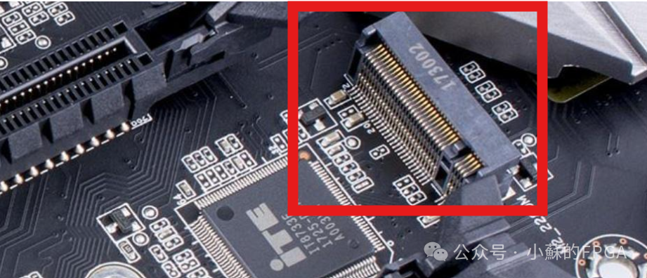
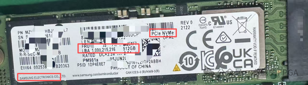
The above image shows the hard drive used in this testing experiment: Samsung, PCIe NVMe 512GB, M.2 interface.
1.2 Application with FPGA
Applying NVMe hard drives on FPGA boards is costly and has a high development difficulty. Some companies specialize in providing NVMe IP cores, priced in the tens of thousands; some individuals or teams also offer NVMe IP cores, priced in the tens of thousands.
1.3 Protocol Introduction
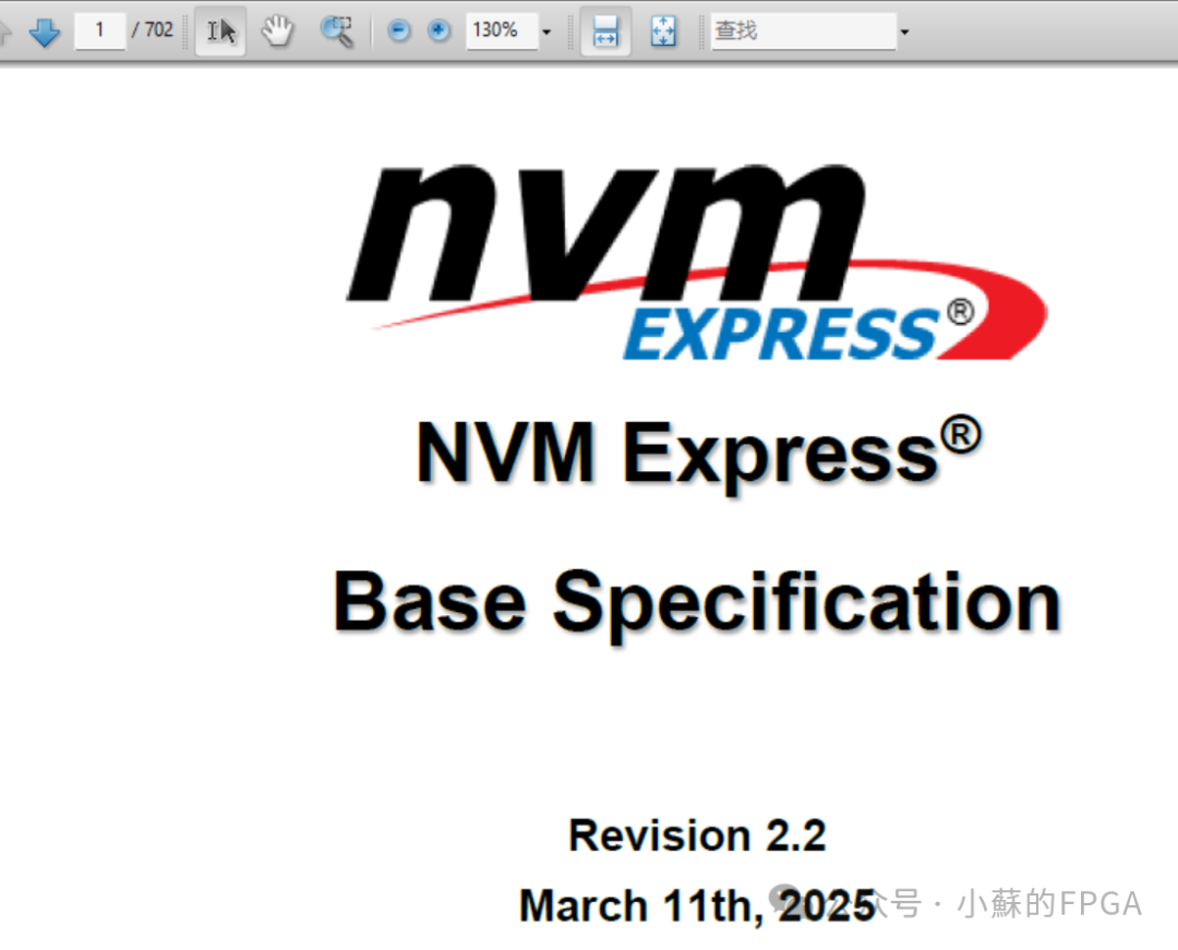
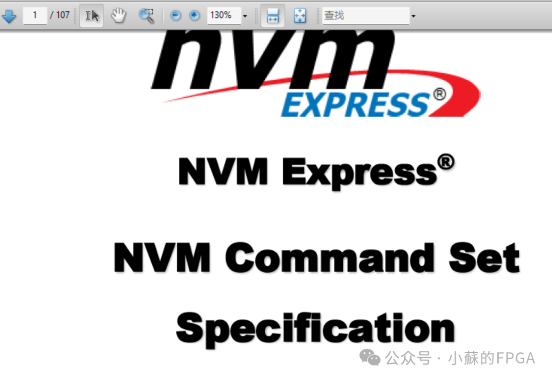
There is a lot of relevant protocol content, and the following literature can be referenced for NVMe-related information: such as queues, commands, PCIe RC, etc. The NVMe protocol is essentially implemented based on the encapsulation of PCIe TLP.

There is also a lot of content related to NVMe protocols and command definitions:
2. Hard Drive Read and Write Testing
Referring to the engineering design from Hanyang University: testing incremental data after DDR caching, configuring and creating queues, and submitting to write into the NVMe hard drive; under read test enable, reading test data from the NVMe hard drive to DDR, then reading test data from DDR and comparing whether there are errors.
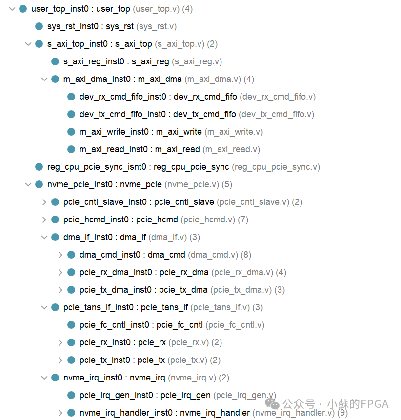
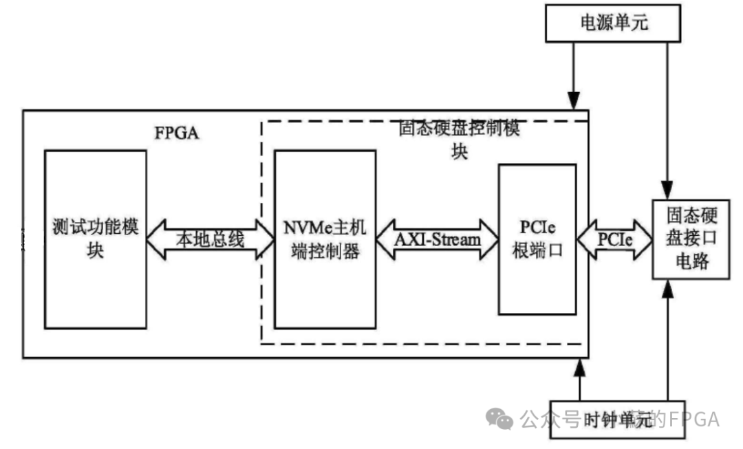
Due to the high cost of testing, this time the Samsung drive was used for testing, and the results are as follows (not considering factors such as temperature): creating a queue for a read and write test.
| Test Capacity (GB) | Write Speed (MB/S) | Read Speed (MB/S) |
| 1GB | 1317 | 2353 |
| 10GB | 976 | 2401 |
| 50GB | 853 | 2401 |
| 100GB | 658 | 2400 |
The above test results are consistent with other literature and tests, with read speeds faster than write speeds. As the write length of the created and executed queue increases, the write speed decreases.
2.1 Read and Write 1GB Speed Test
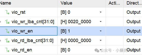
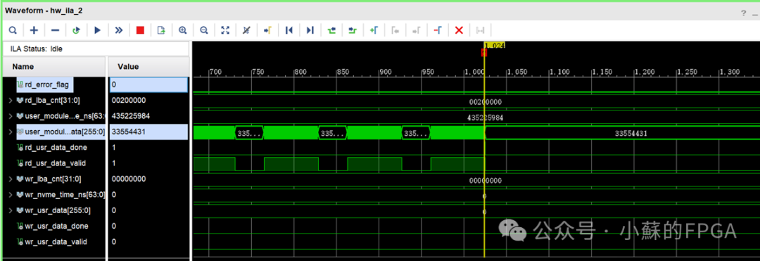
The number of LBAs (512B) corresponding to 1GB is 0x00200000. Set read and write enable, capture the read and write hard drive time and error flags:
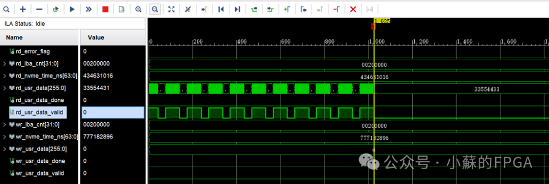 As shown in the figure: the time required to write 1GB capacity to the hard drive is 777182896ns, and the time required to read 1GB capacity is 434631016ns, with no error codes. The write speed is approximately 1317MB/S, and the read speed is approximately 2356MB/S.After the board is powered off and restarted, the time required to read 1GB capacity is 435225984ns,with a read speed of approximately 2353MB/S..
2.2 Read and Write 10GB Speed Test
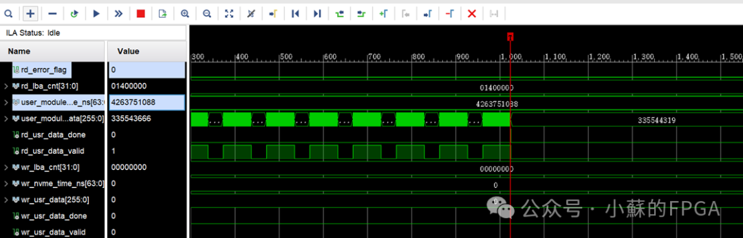
Set read and write LBA to 0x01400000
The time to write to the hard drive is 10489955160ns, with a write speed of: 976MB/S;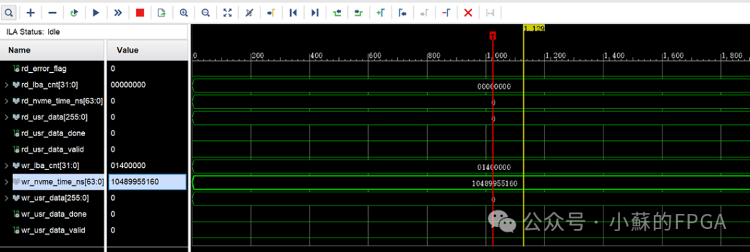
The time to read from the hard drive is 4263751088ns, with a read speed of 2401MB/S;
2.3 Read and Write 50GB Speed Test
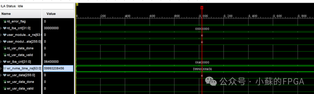
The time required to write 50GB is: 59993208456ns, with a write speed of: 853MB/S.
The time required to read 50GB is: 21318613408ns, with a read speed of: 2401MB/S.
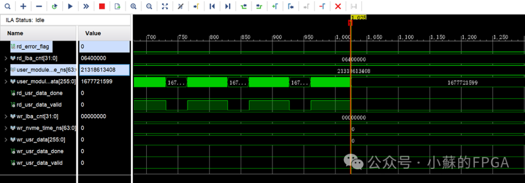
2.4 Read and Write 100GB Speed Test
The time to write 100GB is 155584227432ns, with a write speed of: 658MB/S.
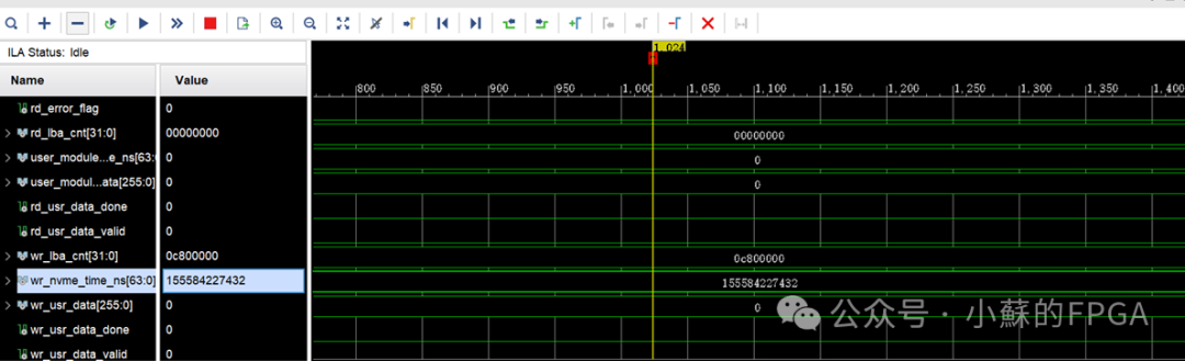
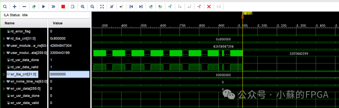
The time to read 100GB is 42654847304ns, with a read speed of: 2400MB/S.
 PreviousHighlightsReviewSeries on the Use of JESD204B – 2, Protocol and ADC Applications (AD9689)FPGA Implementation of 100G UDP CommunicationFPGA-based SRIO Communication (Nwrite+Doorbell)FPGA Implementation of File Read and Write Functionality on SD Cards (FAT32 File System)FPGA Implementation of Gigabit Ethernet UDP Protocol (including ARP, ICMP)Remote Update Function Based on ZYNQFPGA Implementation of Aurora Optical Communication ApplicationsBroadband Signal Multi-phase Filtering and Pulse Compression Processing (FPGA+ADC)FPGA-based AES128 Encryption and Decryption Implementation
Follow us to learn more exciting content

 Share, like, and arrange to see?