

In surface mount technology (SMT), internal voids in solder joints are one of the main defects affecting the reliability of electronic components. Voids can weaken the mechanical strength, conductivity, and thermal conductivity of solder joints, which may lead to catastrophic failures, especially in high-reliability fields such as automotive electronics and aerospace. This article systematically analyzes the core factors causing void formation during the SMT soldering process, covering multi-dimensional reasons including materials, processes, designs, and environmental factors, providing a scientific basis for void control.

1. Material Factors
1. Solder Paste Composition and Properties
1) Alloy System:
Traditional lead-free alloys (such as SAC305) have a high solidification shrinkage rate (approximately 4%), making them prone to micro-voids during the cooling phase.
Low-shrinkage alloys containing elements like Bi and In (such as SnAgCuBi) can reduce shrinkage stress and lower void rates.
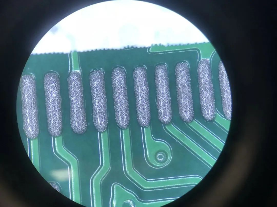
2) Flux Performance:
Volatility Rate: If the flux solvent evaporates too quickly (e.g., high boiling point solvents not fully expelled), it can lead to gas retention;
Residual Activator: Gases such as CO₂ and H₂O generated from the decomposition of acidic activators, if not released in time, will form voids;
Viscosity and Thixotropy: High viscosity solder paste has poor flowability, hindering gas expulsion (IPC J-STD-005 standard requires viscosity range: 150-250 Pa·s).
2. Solder Paste Storage and Usage
1) Solder paste exposed to humid environments absorbs moisture, causing vapor bubbles during reflow;
2) The activity of the flux in solder paste exceeding its shelf life decreases, leading to insufficient wetting and gas retention.
2. Process Parameter Factors
1. Printing Process
1) Stencil Design:
Insufficient matching between the opening size and the PCB pad (e.g., opening area ratio < 0.66) leads to incomplete solder paste release;
Excessively thick stencils (>150μm) can cause solder paste collapse, trapping gas.
2) Printing Parameters:
Excessive squeegee pressure (>8kg) compresses solder paste into the stencil wall gaps, forming micro-bubbles;
Printing speed too fast (>50mm/s) leads to uneven solder paste filling.
2. Placement and Reflow Soldering
1) Component Placement Pressure:
2) Reflow Temperature Curve:
Excessive preheating rate (>3℃/s) triggers rapid flux volatilization, preventing gas from escaping;
Insufficient time above liquidus (TAL) (<60s) leads to inadequate gas escape time;
Excessively high peak temperature (>250℃) exacerbates metal oxidation, generating oxide inclusions.
3. Environmental Control
1) Excessive workshop humidity (>60% RH) causes PCB or components to absorb moisture, generating steam bubbles during reflow;
2) Insufficient nitrogen protection (oxygen content >1000ppm) increases solder oxidation, raising void risk.
3. Design and Equipment Factors
1. PCB and Pad Design
1) Pad Size:
2) Heat Dissipation Design:
3) Solder Mask Window:
2. Component Packaging Type
1) BGA/CSP Packaging:
2) QFN Packaging:
4. Typical Case Analysis
Case 1: BGA Voids Exceeding Standards in Automotive ECU Module
Phenomenon: Void rate 15% (requirement <10%);
Cause:
Stencil opening designed as 1:0.9 (pad: opening), insufficient solder paste volume;
Nitrogen purity in the reflow oven was only 98% (target >99.99%), exacerbating oxidation;
Improvement: Adjusted opening to 1:1.1, after upgrading the nitrogen system, void rate dropped to 7%.
Case 2: Concentrated Voids in LED Power Module
Phenomenon: Voids concentrated in the heat dissipation pad area;
Cause:
Thermal capacity difference between FR4 substrate and copper layer caused rapid heat dissipation;
Improvement: Adopted a stepwise reflow curve, extended TAL time in the heat dissipation area, void rate decreased by 40%.
5. Void Control Strategies
1. Material Selection: Prefer low void rate solder paste (such as SAC+ series with nano-additives);
2. Process Optimization:
1) Set “slow heating – long holding – slow cooling” reflow curve (see Figure 1);
2) Vacuum reflow soldering for key components (void rate can be reduced to below 1%);
3. Design Specifications:
1) Design stencil openings according to IPC-7525 standard (area ratio ≥0.66);
2) Add exhaust channels for large pads (e.g., cross-sectional design);
4. Detection and Monitoring:
1) Use 3D X-ray inspection (resolution ≤5μm) with Sensi 3D X-ray inspection equipment;
2) Real-time SPC statistical process control (e.g., CPK ≥1.33).
Conclusion
Void formation in SMT soldering is the result of the combined effects of material properties, process parameters, design specifications, and environmental factors. By systematically optimizing alloy composition, flux formulation, printing/reflow processes, and PCB design, the void rate can be significantly reduced. With the development of AI-driven process simulation and online detection technologies, real-time prediction and closed-loop control of voids are expected to be achieved in the future, further meeting the needs of high-reliability electronic manufacturing.
Come scan the QR code below to register for free and visit the 2025 Munich Shanghai Electronic Production Equipment Exhibition, skip the queue and get in faster!
Come scan the QR code below to register for free and visit the 2025 Munich Shanghai Electronic Production Equipment Exhibition, skip the queue and get in faster!Technology is the foundation of national strength,
Innovation is the soul of national progress,
Smart businessmen are promoting through SMT headlines.
Low-cost reach to tens of thousands of precise SMT factories,
Making business cooperation easier!
Click the original text to register for the exhibition.