JTAG (Joint Test Action Group) is an international standard testing protocol (IEEE 1149.1) primarily used for testing, debugging, and programming chips, PCBs, and systems. Through a dedicated hardware interface and protocol, it provides non-intrusive access to the internal circuits of chips. The JTAG protocol is widely used in embedded development, hardware verification, and fault diagnosis. This article mainly introduces common application scenarios of the JTAG protocol in chip ATE testing and analyzes the main failure models.
- Introduction to JTAG Module and PIN Functions
The JTAG module generally uses 4 or 5 essential signals to interact with other systems. The common PINs and their function descriptions of JTAG are shown in the figure below:
|
Signal Name |
Direction |
Function Description |
|
TMS |
Input |
Test mode select, controls the TAP state machine switching. |
|
TCK |
Input |
DUT test clock, used for data synchronization between different systems. |
|
TDI |
Input |
Test data input, serial input instructions/data. |
|
TDO |
Output |
Test data output, serial output data. |
|
TRST |
Input |
(Optional) JTAG state machine reset signal. |
According to the IEEE 1149.1 standard document, the internal functional module display of the JTAG system is shown in the figure below: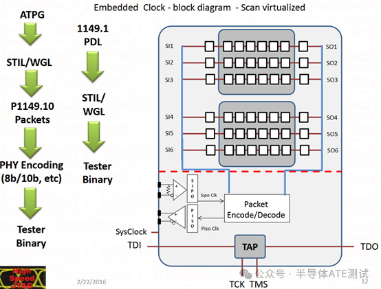 As shown in the figure above, the JTAG interface mainly consists of three parts: the TAP state machine, the encoder/decoder, and the scan chain:1. State Machine – TAP Controller (Test Access Port Controller): The core component of JTAG, controls the internal data flow of JTAG through the TMS signal. There are 16 controllable signal states for TMS (common ones include: Shift-IR, Shift-DR, Run-Test, etc., refer to the IEEE 1149.1 standard document for details).2. Encoder/Decoder (Packet Encode/Decode): The encoder/decoder mainly consists of the Instruction Register (IR) and Data Register (DR).
- Instruction Register – IR: Selects the operation type (e.g., BYPASS, SAMPLE, EXETEST) to control the data register.
- Data Register – DR: Stores specific data (e.g., scan data chain, debug instructions, etc.), controlling the observation of chip input and output.
3. Scan Chain: Different IP DFT scan chains can be connected in series to form a chain, accessed sequentially through TDI -> TDO. To accurately locate Pass/Fail IPs, each JTAG-connected IP needs a unique ID identifier.
- Application of JTAG in ATE Testing
In chip ATE (Automatic Test Equipment) testing, JTAG is a key technology for DFT (Design for Testability) test vectors, which can improve test coverage, reduce test costs, and the JTAG interface can also support mass production testing of complex chips. The following are specific applications and implementations of JTAG in chip ATE and DFT testing. The figure below illustrates the testing principles of JTAG in DUT (Device Under Test) DFT testing.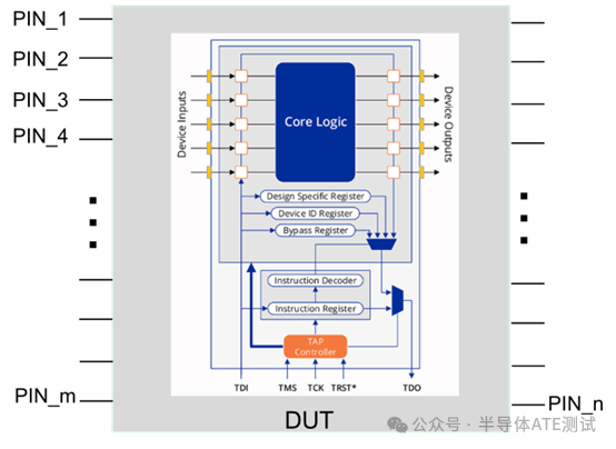
Common applications of JTAG in chip DFT testing include: Boundary Scan Testing (Bscan), Internal Logic Testing (InTest), and Built-In Self-Test (BIST).
-
Boundary Scan Testing
Utilizes the JTAG protocol to control the internal IP interconnections of the chip, forming a test link with I/O pin units through 4 or 5 JTAG pins to complete the testing of hundreds of internal I/Os and Mux interconnections. This improves chip testability and saves ATE testing resources.
-
Built-In Self-Test (BIST)
Can trigger the chip’s internal BIST logic (such as Memory BIST, Logic BIST) through JTAG testing and read the test results.
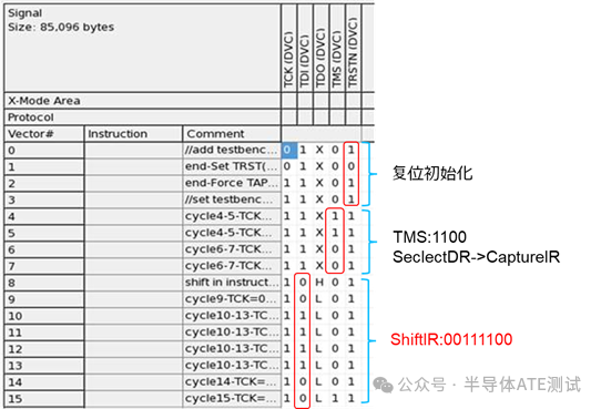
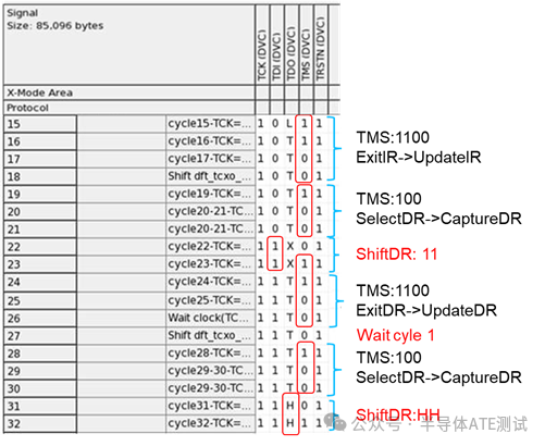
Bscan configuration Pattern example -93K (BIST configuration mode is similar).
-
Internal Logic Testing (InTest)
Implements internal logic testing of the chip (such as registers, memory, and deeply embedded CPU cores) through JTAG, replacing traditional ATE chip logic vector testing. Its advantages include reducing the demand for ATE test channels, thereby lowering testing costs.
-
Common Failure Models in JTAG DFT Patterns
1. Scan Chain Break or Misalignment
-
Symptoms:
-
ATE reading IDCODE failure, or scan chain length does not match expectations.
-
During Pattern execution, output capture data is all 0s/1s or random noise.
-
Possible Causes:
-
Design issues: Scan chain not correctly inserted (DFT tool configuration error).
-
Manufacturing defects: Scan cell or link wire short or open circuit.
-
Packaging issues: JTAG pin cold solder or bond wire breakage.
2. Clock (TCK) or Control Signal (TMS) Issues
-
Symptoms:
-
TAP controller state machine cannot transition normally (e.g., stuck in Reset state).
-
Data shifting errors lead to Pattern comparison failures.
-
Possible Causes:
-
TCK frequency exceeds chip specifications (ATE clock configuration error).
-
TMS signal timing violations (insufficient setup/hold time).
-
Poor signal integrity (reflection, crosstalk, ground bounce noise).
3. Boundary Scan Failure
-
Symptoms:
-
In EXETEST mode, input/output pin levels do not meet expectations.
-
SAMPLE/PRELOAD instructions cannot correctly capture pin states.
-
Possible Causes:
-
Boundary scan cell not correctly inserted or connected.
-
PCB interconnection issues (e.g., open circuit, short circuit).
-
Test vector generation errors (e.g., not covering all BSC).
4. Built-In Self-Test Failure
-
Symptoms:
-
In INTEST mode, internal register read/write anomalies.
-
After executing RUNBIST instruction, BIST results are incorrect.
-
Possible Causes:
-
Test logic (e.g., BIST engine) not correctly integrated.
-
Clock domain crossing (CDC) issues causing signal desynchronization.
-
Test vectors not covering target logic paths.
5. Multi-Device Chain Synchronization Issues
-
Symptoms:
-
Some devices in the chain are unresponsive, or IDCODE order is incorrect.
-
Data shifting interference in the chain (e.g., TDO signal crosstalk).
-
Possible Causes:
-
Device scan chain length configuration error (ATE does not match design).
-
Some device JTAG interface disabled (e.g., fuse bit programming error).
6. Power Environment Sensitivity Issues
-
Symptoms:
-
Pattern failure under high/low temperature or low voltage.
-
Random errors (e.g., sporadic TDO data errors).
-
Possible Causes:
-
Power noise causing JTAG signal jitter.
-
Temperature drift affecting TCK timing.
-
Common Debugging Thoughts and Steps:
1. Isolate Hardware Issues
-
Confirm whether the chip’s JTAG-related PINs are correctly connected (PerPin PMU test related channel OS value, note that the PINs ac relay should be disconnected).
-
Check the chip’s power supply status (using an oscilloscope/multimeter to capture the actual power waveform/power voltage value at PowerUp).
-
Confirm the current Pattern configuration (system).
-
Scan mode (BIST pattern test),
-
Extest Mode (external test mode: commonly used for Bscan Pattern test),
-
Function mode (SLT test, delivered to customers for normal use).
-
When conditions permit: swap chips, LB/PC, test machines, to eliminate the impact of test hardware on test results.
2. ATE Failure Pattern Analysis Tools
-
When capturing FailCycle on ATE machines, pay special attention to the first failure point. The DFT department can locate which Scan Cell is abnormal based on the FailCycle, and provide the related Pin List and failure model for that Scan Cell, as well as debugging ideas (this can be further localized using the first two steps in “Isolate Hardware Issues”).
-
Collaborate with DFT colleagues to split Patterns, gradually narrowing down the problematic IP range. This can also eliminate the impact of internal IR Drop on Pattern test results (to reduce testing costs, a single Pattern often contains multiple IP Test cells; when a failure occurs, splitting the Pattern can help us quickly confirm the specific failing IP).
-
Raise the input voltage settings for the TDI PIN in the test program, relax the TDO PIN voltage settings (to eliminate the impact of ATE-related hardware on pattern test results).
-
Relax test period, confirm whether it is stack fail or transition fail.
-
Burst setup pattern and Scan pattern, eliminate failures caused by test suit switching leading to clock restarts.
-
Modify system clock duty cycle, eliminate failures caused by insufficient DUT system clock tree margin.
-
Use Timing Diagram to analyze key PIN waveform diagrams.
JTAG is an indispensable technology in chip ATE and DFT testing. It significantly enhances testing efficiency and coverage through boundary scanning and standardized interfaces. For DFT engineers, rationally designing JTAG chains and instruction sets is crucial; for ATE engineers, mastering the integration of JTAG protocols and test programs is essential. As chip complexity increases, the integration of JTAG with BIST, SCAN, and other technologies will become even closer.