In mid-2022, Renesas Electronics announced the completion of its acquisition of Transphorm. In the FY2024 annual report, Renesas discussed the purpose of the acquisition: based on Transphorm’s capabilities in the GaN field, and industry research indicating that the GaN market demand is expected to grow at an annual rate exceeding 50%, “the company will adopt Transphorm’s auto-qualified GaN technology to develop new advanced power solutions, such as multi-in-one (X-in-1) power system solutions for electric vehicles, as well as applications in computing, energy, industrial, and consumer sectors.”
The acquisition of Transphorm by Renesas also aligns with public expectations. Industry opinions generally believe that the GaN market is moving towards consolidation; and from the increasingly frequent actions of market participants like Renesas and Infineon, the competition in the GaN market is also testing vertical integration capabilities—mergers and acquisitions have thus become inevitable.

At a recent product launch, Kenny Yim, Senior Director of GaN/Power at Renesas, also mentioned the intense competition in the GaN market, prompting Renesas to focus on innovations in GaN “Gen IV Plus” technology to achieve further improvements in performance, stability, flexibility, and cost-effectiveness, thereby gaining an advantage in competition.
This launch primarily features new products based on its fourth-generation enhanced GaN technology, specifically a 650V 30mΩ GaN FET aimed at AI data center power supplies, UPS, solar inverters, battery storage converters, electric vehicle charging, automotive OBC, and DCDC applications. Through this product launch, we can glimpse Renesas’ differentiated competitive capabilities and future plans for GaN products following the acquisition of Transphorm.
Differentiation: GaN FETs for High Power Applications
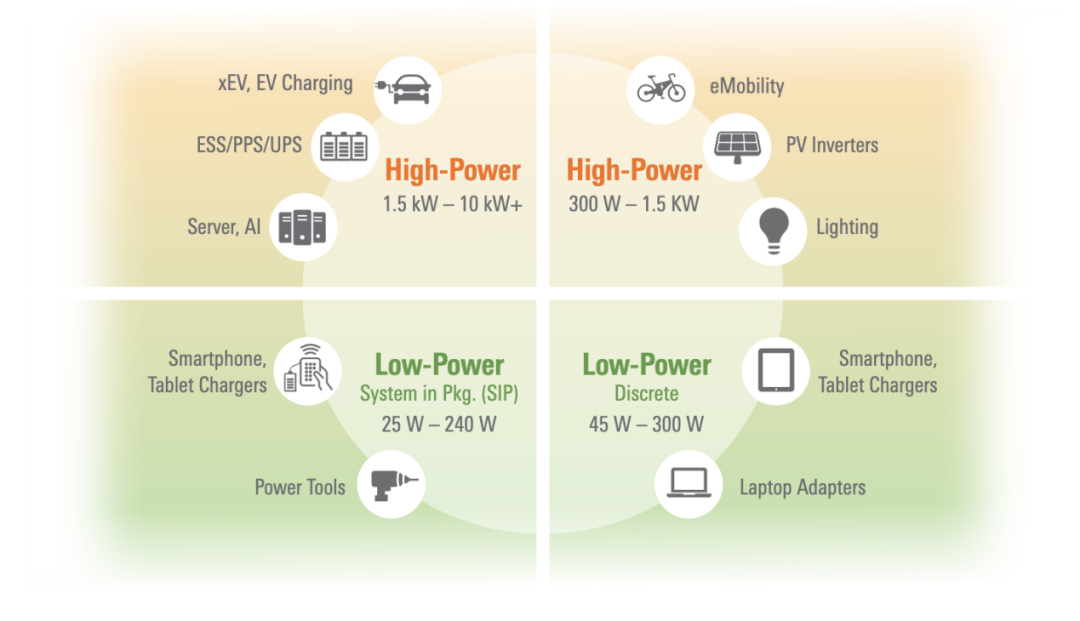
Readers who focus on Si (silicon), SiC (silicon carbide), and GaN (gallium nitride) switching device technologies and markets should generally know that compared to traditional silicon-based power devices, SiC can balance switching frequency and power density; GaN’s advantage lies in achieving higher switching frequencies, but generally, its power range coverage is not particularly wide—especially in the high power range, which is still more within SiC’s reach.
However, Kenny specifically mentioned that a significant feature of Renesas’ GaN technology is that “from high power applications of 6kW to 12kW, down to low power applications of several watts, our GaN devices support both,” thus for “electric vehicle motor drives and OBC charging, we can also provide high power GaN devices.”
“There is a misconception in the market that GaN is only used for low power applications. However, we have been applying GaN in data center servers, automotive OBC, and other applications since 2012.” In a market where most competing GaN devices are only suitable for low power applications, “the ability of GaN products to be applied in high power scenarios” is one of Renesas’ most important differentiating capabilities.
Kenny further clarified during the media Q&A session that Renesas positions its GaN products “for the market below 1200V,” and compared to SiC MOSFETs, there will be significant cost advantages: although in some applications, “the volume has not yet matured enough to pose a significant cost advantage over SiC devices, but that is just around the corner.” (2) In terms of performance, switching losses are much lower than those of SiC MOSFETs, “because there is no body diode, and there is no reverse recovery loss,” thus GaN devices have an advantage in overall conversion efficiency.
The main reason Renesas’ SuperGaN products can be used in high power applications is naturally due to the device being based on a D-mode (depletion-mode) structure. We know that D-mode GaN devices are normally-on by default, requiring either a negative voltage at the gate to turn them off or a cascode structure to switch them to a normally-off state—”we control the switching with a MOSFET,” which is the concept behind SuperGaN’s D-mode operation.
Generally speaking, D-mode GaN has significant advantages in robustness, high-speed switching, and thermal stability—when supported by a cascode structure, it can adapt to automotive, industrial, and other high power systems. Kenny discussed the defects of E-mode (enhancement-mode) GaN during the media session:
Due to the p-GaN gate structure of E-mode GaN, its low Vgs characteristics make it incompatible with conventional drivers and highly sensitive to parasitic inductance, limiting its application in TO-220, TO-247, and other pin packages; at the same time, limited by gate drive voltage, the saturation drain current (Idsat) is relatively low, and the current capability decreases significantly with increasing temperature.
Additionally, the p-GaN structure introduces extra gate capacitance and driving bottlenecks, making the device’s performance in high-frequency switching scenarios inferior to that of D-mode GaN; it is also prone to issues such as increased dynamic on-resistance (RDs(on)), excessive reverse conduction voltage drop (Vsd), and so on…
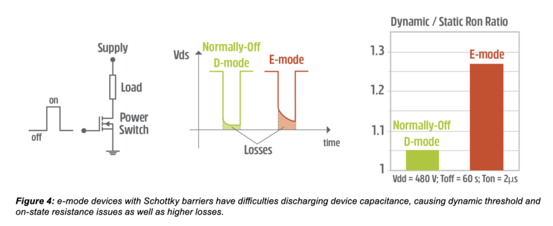
Source:The Fundamental Advantages of Normally-Off D-Mode GaN, Renesas
The defects of E-mode GaN naturally make it difficult to adapt to high power and high temperature applications. In contrast, Renesas’ D-mode GaN products, due to their structural characteristics, have significant advantages in efficiency and reliability compared to E-mode GaN—especially the cascode structure brings gate robustness and reliability, as well as relatively low cost. These are the technical foundations that allow Renesas’ SuperGaN to be used in high power applications.
Kenny added, “The key technology of D-mode is controlling D-mode GaN devices with a MOSFET. This is Renesas’ patent,” and currently unique to Renesas—this refers to the technology related to the cascode structure. The patent comes from the original Transphorm, and in 2023, Renesas provided awhite paper on the advantages of cascode structure D-Mode GaN technology from Transphorm, which interested readers can download and read.
“We are not the only ones making D-mode GaN,” but limited by patents, most other competitors “can only use ICs for driving”; at the same time, “we have also licensed this patent to some partners,” so the market will also see other products based on Renesas’ cascode structure D-mode GaN-related patents. This patent is likely to remain a key factor in Renesas’ competition in the high voltage, high power GaN market for a considerable time; it is also a core element for Renesas’ SuperGaN to pass AEC-Q101 certification and be used in automotive applications.
However, Kenny also mentioned that Renesas is not only making D-mode GaN products; they also plan to launch low voltage GaN based on E-mode structure in the future. “Our company is currently working on both E-mode and D-mode technology products.” “However, because we believe that E-mode has many shortcomings in high voltage applications at this stage, we will not push high voltage E-mode GaN for now.”
Launch of Three New 650V 30mΩ Products
In fact, this type of product has already been applied in high power applications including data centers (various PSUs, UPS, etc.), solar micro-inverters, and even gaming PC power supplies, “including the currently popular ROG power supplies available on JD.com.” “These high power applications, reaching up to 7.5kW, have not yet seen any E-mode GaN companies able to provide mass production cases for customers.”
Specifically regarding the new products, based on the aforementioned technical characteristics, Renesas has launched three high voltage 650V GaN FETs, namely TP65H030G4PRS, TP65H030G4PWS, and TP65H030G4PQS, offering TOLT, TOLL, and TO-247 packaging options—achieving better versatility. Kenny mentioned that there will be other packaging options in the future, “providing a wide range of packaging options for power systems from 1kW to 10kW.”

The target applications for the new products cover AI data center server power supplies—Renesas particularly mentioned 800V HVDC architecture, electric vehicle charging, automotive OBC and DCDC, battery storage, solar inverters, etc. AI, automotive, and new energy are always the focus of mainstream market competitors—especially as Kenny mentioned, “We are providing AC to DC efficiency of 98.3% power reference solutions to leading companies in the AI field, including Company N”—”This is a 230V to 54V 6.6kW platform, which is already a relatively mature solution.”
“These are currently the largest markets, so we are launching the 30mΩ new products to replace the previous generation 35mΩ products.” Kenny stated that based on the fierce competition in the current GaN market, Renesas is taking the lead in launching these GaN new products aimed at applications that can generate volume and revenue, “lower voltage, smaller power products will also be developed in the future”; meanwhile, it is said that even higher voltage products, such as 1200V, are also in the pipeline.
Some important features of the new products listed by Renesas include (1) the new generation GaN FET achieves efficient, high power density, and reliable power conversion for kilowatt-level applications; (2) broad support for TO and SMT packaging;
(3) the Normally-off D-mode architecture (i.e., based on cascode structure D-mode) achieves compatibility with standard silicon drivers, creating a more direct and cost-effective GaN adaptability; (4) better noise immunity compared to E-mode, avoiding false turn-on caused by gate transients; (5) parallel operation > 7.5kW. Most projects have also more concretely described the capabilities achieved by the aforementioned Renesas patented technology.
Additionally, it is worth mentioning that the process-related “Gen IV Plus” platform has made progress in performance and cost compared to the previous fourth generation (Gen IV). Including the current 30mΩ compared to the previous 35mΩ product, RDs(on) and die size have achieved approximately a 14% reduction—correspondingly achieving cost reduction; FoM (Figure of Merit) improved by up to 50% (Ron x Qg improved by up to 50%, Ron x Qoss improved >20%), long-term reliability enhanced; the widest range of packaging types supported, achieving better flexibility.
Kenny even specifically compared the newly released products with 650V 33mΩ SiC MOSFETs (at 66kHz) during the media session, “In terms of efficiency in totem pole PFC, the new products are 0.2 points higher than SiC. This 0.2 points is significant because when everyone is achieving around 99% efficiency, being 0.2 points higher means a 20% reduction in losses.” “If the frequency is further increased, the advantage will be even greater.” This also reflects the faster switching frequency, giving GaN an advantage over SiC in specific applications, while also being relatively lower in cost.
Further Leveraging Renesas’ Advantages
Beyond devices and chips, creating a more complete system and offering comprehensive solutions to users is a strong suit of market participants like Renesas. In recent years, leading companies, including Renesas, have been particularly aggressive in covering more complete signal chains and pushing more comprehensive product offerings. This is also the fundamental logic behind the continuous mergers, acquisitions, and R&D investments by large enterprises targeting key nodes in the signal chain, including Renesas’ acquisition of Transphorm.
After acquiring Transphorm, Renesas’ vertical integration supply chain layout in the GaN device field includes: (1) mastering the design capabilities of GaN FETs, (2) “we also do the epitaxy ourselves”;
(3) based on existing silicon wafer manufacturing fabs, including Renesas’ own and joint ventures with partners—currently, Renesas has a 6-inch wafer fab in Japan, with plans to expand to an 8-inch fab by 2027, and also collaborates with external foundries for 8-inch wafer manufacturing—this April, Polar Semi announced a licensing cooperation with Renesas regarding D-mode GaN-on-Si technology, where Polar will be responsible for manufacturing high voltage 650V GaN devices for Renesas and its customers;
(4) packaging mainly adopts external OSAT; (5) moving towards the application side, providing customers with a complete ecosystem and reference designs is also standard practice for Renesas.
As for specific applications, Kenny listed SuperGaN’s use in high voltage bus-level AC-DC conversion for AI data centers, as well as stepping down ±400V DC to 48-54V for server supply—this is likely closer to the reference solution Kenny mentioned for Company N. However, beyond GaN FETs, Renesas’ advantages are still reflected in the support of various products, including MCUs, drivers, controllers, and other power components and modules. “In addition to MOSFETs as switching devices, Renesas also provides a complete solution, including MCUs, PWM, gate drivers, etc.; from totem pole PFC to LLC, BMS, DCDC, and so on.”
Renesas’ Vice President of GaN Business, Primit Parikh, stated: “In the future, we will deeply integrate the market-validated SuperGaN technology with Renesas’ rich lineup of driver and controller products, aiming to create complete power solutions.” Renesas’ previously emphasized “one-stop” service, and the concept of an ecosystem (GaN + IC + solutions) and Winning Combo will undoubtedly also be reflected in GaN products.

“We are targeting the AI data center and industrial markets, with high power density (>100W/in³) and efficiency advantages; for automotive applications, we also have high frequency (>100kHz), energy-saving, efficient, and smaller size characteristics.” Kenny summarized: “We hope to provide customers with energy-saving, comfortable, and cost-effective power products and power conversion systems.”
By integrating the patented technology of the original Transphorm in cascode structure D-mode GaN devices, achieving technological advantages also allows GaN to expand into a wider range of applications. Coupled with Renesas’ vertical integration capabilities and the provision of complete system-level solutions to applications and customers, Renesas has maintained considerable initiative in today’s market hotspots, including automotive, AI, and new energy—although GaN is just one aspect of it.
It is worth mentioning that Renesas has indicated in its PPT that its GaN products will cover a range from 25W to 100kW, and from 25V to 1200V—implying that more GaN products are already in the pipeline.