Click on the above “Visual Learning for Beginners” to select “Star” or “Top”
Essential insights delivered first-hand
The core of a typical image sensor is the CCD unit (charge-coupled device) or standard CMOS unit (complementary metal-oxide semiconductor). CCD and CMOS sensors have similar characteristics and are widely used in commercial cameras.
However, most modern sensors use CMOS units mainly for manufacturing considerations. Sensors and optical components are often integrated to produce chip-level cameras, which are used in fields such as biology or microscopy, as shown in Figure 1.
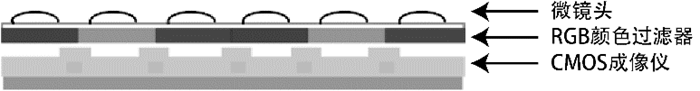
Figure 1: Common arrangement of image sensors integrated with optical components and color filters
Image sensors are designed to meet specific goals for different applications, providing varying levels of sensitivity and quality.
Silicon-based image sensors are the most widely used, though other materials may be employed, such as gallium (Ga) for longer infrared wavelengths in industrial and military applications.
The resolution of image sensors varies across different cameras. From single-pixel phototransistor cameras (used for industrial applications via a one-dimensional linear scanning array) to two-dimensional rectangular arrays on regular cameras (all paths leading to spherical alignment are used for high-resolution imaging), various configurations are possible.
Standard image sensors are manufactured using CCD, CMOS, BSI, and Foveon methods. Silicon image sensors exhibit a nonlinear spectral response curve, which can effectively perceive the near-infrared part of the spectrum but poorly perceive blue, purple, and near-ultraviolet parts (as shown in Figure 2).
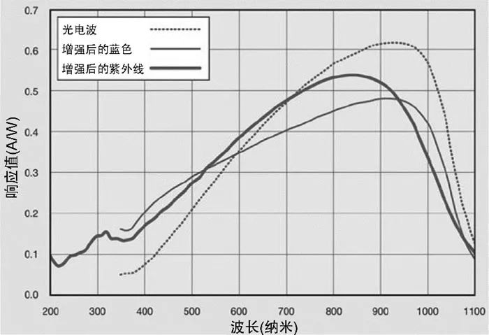
Figure 2: Typical spectral response of several silicon photodiodes
It can be noted that photodiodes exhibit high sensitivity in the near-infrared range around 900 nanometers, while showing nonlinear sensitivity across the visible spectrum of 400 nanometers to 700 nanometers. Due to the standard silicon response, removing the IR filter from the camera increases near-infrared sensitivity. (The use of spectral data images has been authorized by OSI Optoelectronics Co., Ltd.)
Note that when reading raw data and discretizing it into digital pixels, it leads to silicon spectral response. Sensor manufacturers have designed compensations in this area; however, when calibrating camera systems based on applications and designing sensor processing methods, the color response of the sensor should be considered.
The key to image sensors lies in the size of the photodiodes or elements. Sensors using small photodiodes capture fewer photons than those using larger photodiodes.
If the element size is smaller than the wavelength of visible light that can be captured (e.g., blue light at 400 nanometers), then other issues must be overcome in the sensor design to correct the image color. Sensor manufacturers spend significant effort optimizing element size to ensure all colors are represented equally in imaging (as shown in Figure 3).
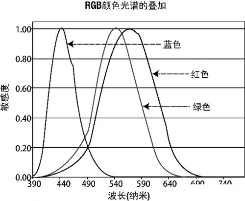
Figure 3: Wavelength distribution of primary colors
Note that the primary color regions overlap, and green is a good monochromatic substitute for all colors.
Figure 4 shows different in-chip configurations of multispectral sensor designs, including mosaic and stacked methods. In the mosaic method, color filters are arranged in a mosaic pattern on each element. The Foveon sensor stacked method relies on the physical penetration of color wavelengths into the semiconductor material, where each color penetrates silicon material to varying degrees, thus imaging their respective colors. The entire element size can be applied to all colors, eliminating the need to configure elements separately for each color.
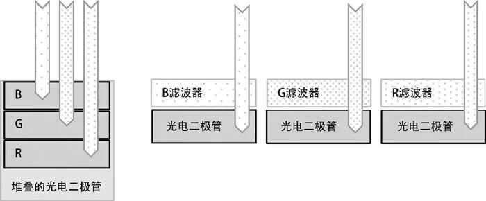
Figure 4: (Left) Foveon method for stacking RGB elements, (Right) Standard mosaic elements
Back-side illuminated (BSI) sensor structures have larger element areas, allowing each element to gather more photons, thus rearranging the sensor wiring on the die.
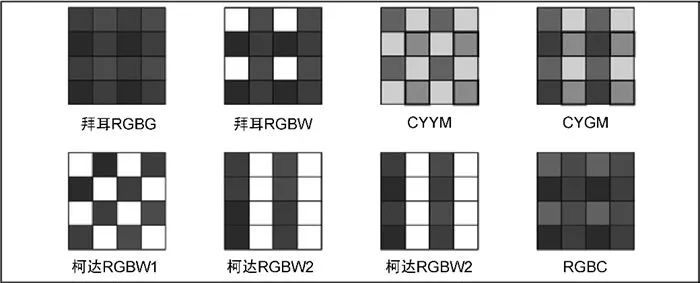
Figure 5: Several different mosaic configurations of element colors, including white, primary RGB colors, and secondary CYM elements
The arrangement of sensor elements also affects color response. For example, Figure 5 shows different arrangements of basic colors (R, G, B) sensors, and white sensors, where the white sensor (W) has a very clear or non-color filter.
The arrangement of the sensor considers a certain range of pixel processing, such as during the processing of pixel information for a sensor, pixels selected from different configurations of adjacent elements are combined, optimizing color response or spatial color resolution.
Currently, the most advanced sensors can provide at least 8 bits per color unit, typically 12 to 14 bits. Sensor elements need space and time to gather photons, so smaller elements must be carefully designed to avoid various issues.
Noise may originate from optical elements used, color filters, sensor elements, gain and A/D converters, post-processing, or compression methods. The readout noise of the sensor also affects actual resolution, as each pixel unit is read from the sensor and sent to the A/D converter to form rows and columns in digital form for pixel conversion. Better sensors produce less noise while achieving higher bit resolution.
Typically, each imaging system contains a proprietary sensor processor, including a fast HW sensor interface, optimized very long instruction word (VLIW), single instruction multiple data (SIMD) instructions, and hardware modules with fixed functions designed to handle the workload caused by large-scale parallel pixel processing.
Generally, the sensor processing is transparent and automated, set by the manufacturer of the imaging system, and all images from the sensor are processed in the same way. There are also other ways to provide raw data, allowing customization of the sensor processing for applications, much like digital photography.
One of the primary challenges of mosaicing is pixel interpolation, which combines the color channels of adjacent cells into a single pixel. This is a significant issue given the geometric shape of the sensor element arrangement and the aspect ratio of the element arrangement. A related issue is the weighting of color cells, such as how much of each color should contribute to each RGB pixel.
Because in mosaic sensors, the spatial element resolution is greater than the final combined RGB pixel resolution, some applications require the raw sensor data to utilize all precision and resolution possible, or some processing may require enhanced effective pixel resolution or better spatially accurate color processing and demosaicing.
Like LCD displays, sensors can also have bad pixels. By providing the coordinates of bad pixels that need correction in the camera module or driver, suppliers can factory-correct the sensor and provide a defect map for known defects.
In some cases, adaptive defect correction methods may be used on the sensor to monitor adjacent pixels for defects and then correct certain types of defects within a range, such as single pixel defects, column or row defects, and similar block defects like 2×2 or 3×3. To find defects in real-time, camera drivers may also provide adaptive defect analysis, and a special compensation control may be available in the camera’s startup menu.
Color correction is necessary to balance overall color accuracy and white balance. As shown in Figures 1-2, silicon sensors are usually sensitive to red and green colors but not sensitive to blue, so understanding and calibrating the sensor is fundamental to achieving the most accurate colors.
The processors of most image sensors contain geometric processors for halo correction, which manifests as darker lighting at the edges of images. The correction is based on geometric distortion functions, considering programmable lighting functions to increase lighting towards the edges, which need to be calibrated before leaving the factory to match the optical halo pattern.
Lenses may have geometric aberrations or distortions occurring towards the edges, resulting in radially distorted images. To address lens distortion, most imaging systems have dedicated sensor processors with hardware-accelerated digital distortion elements, similar to texture samplers on GPUs. Calibration and programming for geometric correction of optical devices are performed at the factory.
Discussion Group
Welcome to join the public account reader group to exchange ideas with peers. Currently, there are WeChat groups for SLAM, 3D vision, sensors, autonomous driving, computational photography, detection, segmentation, recognition, medical imaging, GAN, algorithm competitions, etc. (which will gradually be subdivided in the future), please scan the WeChat ID below to join the group, and note: “nickname + school/company + research direction”, for example: “Zhang San + Shanghai Jiao Tong University + Visual SLAM”. Please follow the format for notes, otherwise, you will not be approved. After successful addition, you will be invited to the relevant WeChat group based on your research direction. Please do not send advertisements in the group, otherwise you will be removed from the group. Thank you for your understanding~