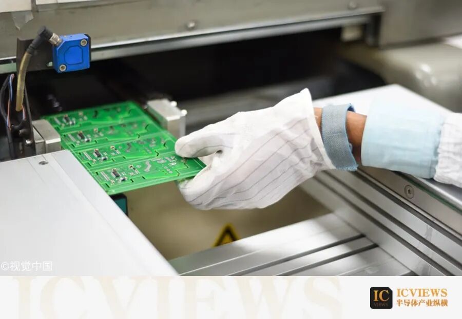
 This article is provided by the Semiconductor Industry Comprehensive (ID:ICVIEWS).STMicroelectronics is building a next-generation panel-level packaging(PLP) technology pilot production line at its factory in Tours, France.
STMicroelectronics (ST) has announced plans to invest $60 million in a new pilot production line for next-generation panel-level packaging (PLP) technology at its factory in Tours, France. The new production line is expected to be operational by the third quarter of 2026.
PLP technology is a method of packaging multiple ICs on a single large rectangular substrate, rather than on a single circular wafer, which increases the number of ICs that can be processed simultaneously, thereby reducing costs and improving yield.
Panel-level packaging has been shown to help reduce production costs for small devices such as smartwatches, power management ICs (PMICs), and Internet of Things (IoT) devices. STMicroelectronics has replaced the lead frame in quad flat no-lead (QFN) packages with a fan-out redistribution layer (RDL), improving production efficiency and reducing costs. The RDL line width/spacing required for such devices is much smaller than the 2/2µm front-end redistribution layer characteristics typically associated with high-performance computing, for example, 10/10µm.
STMicroelectronics plans to leverage its first-generation PLP production line in Malaysia and its global technology R&D network to develop next-generation PLP technology and expand its PLP applications to various products, including automotive, industrial, and consumer products.
Fabio Gualandris, President of Quality, Manufacturing, and Technology at STMicroelectronics, explained: “Our development of PLP technology at the Tours factory aims to advance this innovative chip packaging and testing manufacturing technology, enhancing efficiency and flexibility for widespread applications in RF, analog, power, and microcontroller applications. A multidisciplinary team of experts in manufacturing automation, process engineering, data science and analytics, and technology and product R&D will collaborate on this project. This is an important part of a larger strategic plan focused on heterogeneous integration, a scalable and efficient new method of chip integration.”
 STMicroelectronics’ PLP-DCI Technology
STMicroelectronics’ PLP technology focuses on direct copper interconnect (DCI). DCI replaces traditional wire connections between chips and packaging substrates with high-conductivity copper to electrically connect ICs to the panel substrate. Compared to traditional methods using solder bumps (which may be unreliable), DCI achieves superior performance.
STMicroelectronics explains: “This wireless direct connection technology supports new product development by reducing power loss (e.g., resistance and inductance), improving thermal performance, and shrinking package size, thereby increasing overall power density.” PLP-DCI also supports the integration of multiple chips in system-in-package (SiP) configurations.
STMicroelectronics’ R&D team has been dedicated to prototyping and scaling this technology, achieving a state-of-the-art PLP-DCI process using 700x700mm large panels, and achieving mass production of over 5 million units per day on a highly automated production line.
 TSMC and Other Manufacturers Accelerate FOPLP Technology Development, Reports Indicate Yield Rates Have Reached 90%
TSMC and other semiconductor manufacturers are accelerating the development of fan-out panel-level packaging (FOPLP) technology, which is rapidly gaining industry attention.
According to reports from the Taiwan Commercial Times, supply chain sources indicate that FOPLP equipment has already been shipped, with customer testing yield rates reaching 90%, but large-size applications are still in the “verification and small-scale trial production” stage, with mass production needing to consider risks and costs. The so-called panel-level packaging (PLP) refers to the shift from wafer-level packaging (WLP) that previously used wafers as substrates to using panels as packaging substrates. These substrates can be made from metal, glass, or polymer materials.

The Commercial Times reports that the key to FOPLP is replacing wafers with square panels, compared to wafer-level fan-out packaging (FOWLP), FOPLP uses rectangular substrates, with a 600×600 mm panel area exceeding five times that of a 12-inch wafer, and utilization can be increased from about 57% to 87%, thereby reducing unit costs and enhancing production flexibility.
The industry is adopting a “dual-track” approach. On one hand, FOPLP has entered small-scale mass production, with Innolux and Unimicron leading the way in packaging power management chips (PMICs) and other small chips. On the other hand, TSMC is developing its own CoPoS (wafer-level panel packaging) solution, aiming to support large GPU applications for companies like NVIDIA and AMD, but trial production still faces bottlenecks.
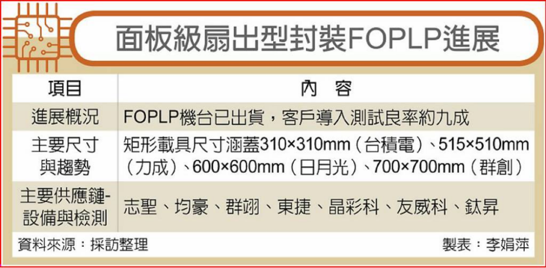
Currently, the substrates used for FOPLP are primarily metal or glass, with mainstream sizes including TSMC’s 310×310 mm, Unimicron’s 515×510 mm, ASE’s 600×600 mm, and Innolux’s 700×700 mm. Reports indicate that Unimicron has achieved a trial production yield rate of 90% after deploying a new generation of laser and dispensing equipment, with expectations to increase to over 95% next year.
In terms of technology layout, TSMC has established a dedicated FOPLP R&D team and production line, investing in PLP (panel-level packaging) and TGV (through-glass vias) to promote the development of glass substrates. The originally planned mass production timeline for 2027 is now expected to be advanced, according to supply chain sources.
Additionally, TSMC confirmed this August that it will phase out 6-inch wafer capacity within two years and consolidate 8-inch capacity to improve efficiency. According to reports from Liberty Times, it is still under evaluation whether TSMC’s wafer fab (6-inch) and fab (8-inch) will be repurposed for advanced packaging, but there are rumors that TSMC may convert them into CoPoS production lines.
*Disclaimer: This article is the original author’s creation. The content reflects their personal views, and our reposting is solely for sharing and discussion purposes, not representing our endorsement or agreement. If there are any objections, please contact us.