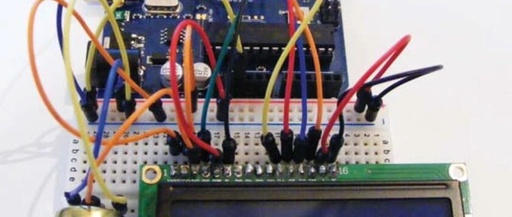
Technology Competition | Our College Achieves Historic Best Performance in Embedded Design Competition
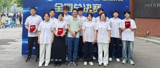
Click the blue text Follow us Technology Competition | Our College Achieves Historic Best Performance in Embedded Design Competition On July 15, 2025, the National Finals of the China College Computer Competition – Embedded Design Competition successfully concluded at Beijing University of Technology. This year’s finals were held offline, gathering 60 top teams from seven … Read more