
1.Overview of Semiconductor Testing and Measurement Equipment
1. Industry Overview
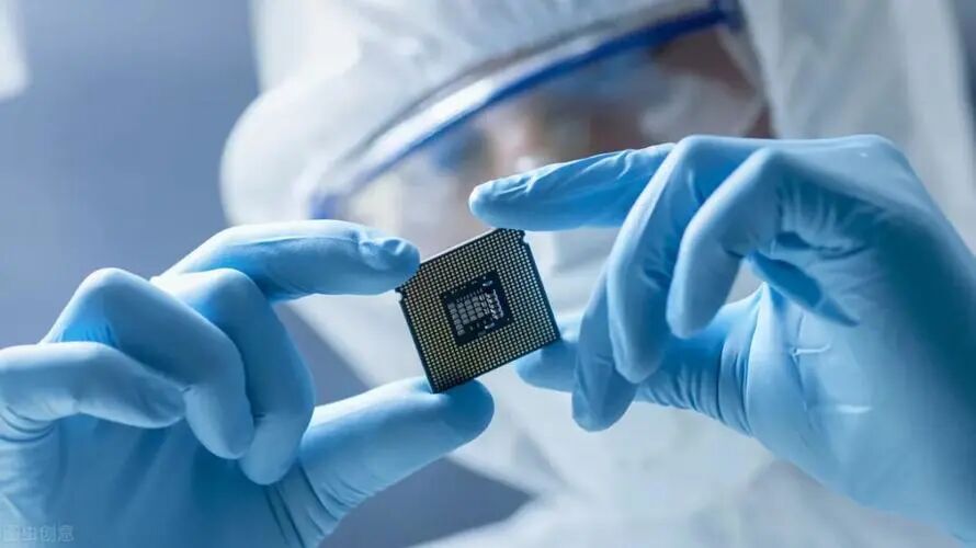
Testing refers to the detection of heterogeneous conditions on the surface of wafers or within circuit structures, such as particle contamination, surface scratches, and open/short circuits, which adversely affect the performance of chip processes due to characteristic structural defects. Measurement refers to the quantitative description of structural dimensions and material properties on the observed wafer circuits, such as film thickness, critical dimensions, etching depth, and surface morphology.
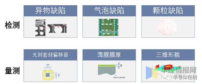
Diagram of testing and measurement applications, Source: ZK Fei Ce Prospectus, Huajing Industry Research Institute
2. Classification Status
From a technical principle perspective, testing and measurement include optical testing technology, electron beam testing technology, and X-ray measurement technology. Currently, among all semiconductor testing and measurement equipment, devices utilizing optical testing technology account for the majority. Optical testing technology is based on optical principles, calculating and analyzing light signals to obtain testing results. During production, optical testing technology is required for detecting issues such as impurity particles and pattern defects on the wafer surface, as well as measuring film thickness, critical dimensions, overlay accuracy, and surface morphology.
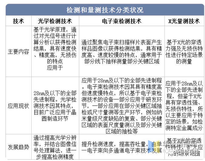
Classification status of testing and measurement technologies, Source: Public data compilation
2. Background of Testing and Measurement Technologies
1. Testing
In the testing phase, optical testing technology can be further divided into non-patterned wafer laser scanning testing technology, patterned wafer imaging testing technology, and photomask imaging testing technology.
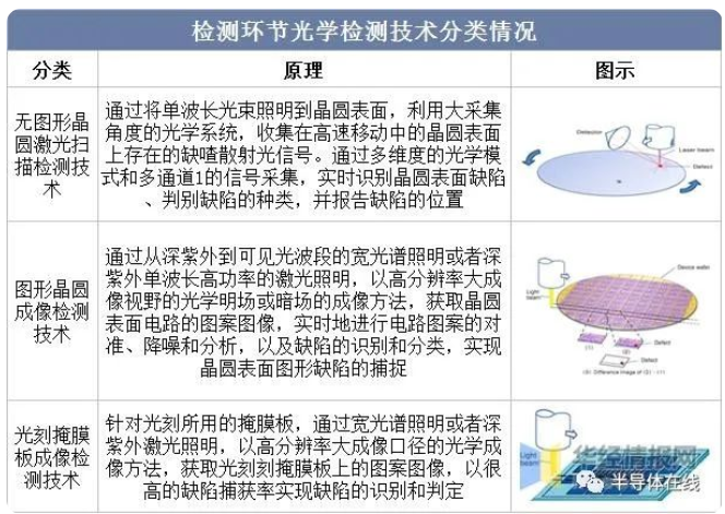
Classification of optical testing technology in the testing phase, Source: Public data compilation
2. Measurement
In the measurement phase, optical testing technology achieves measurements far smaller than the wavelength of light based on the wave nature and coherence of light. Measurement in integrated circuit manufacturing and advanced packaging primarily includes three-dimensional morphology measurement, film thickness measurement, overlay accuracy measurement, and critical dimension measurement.
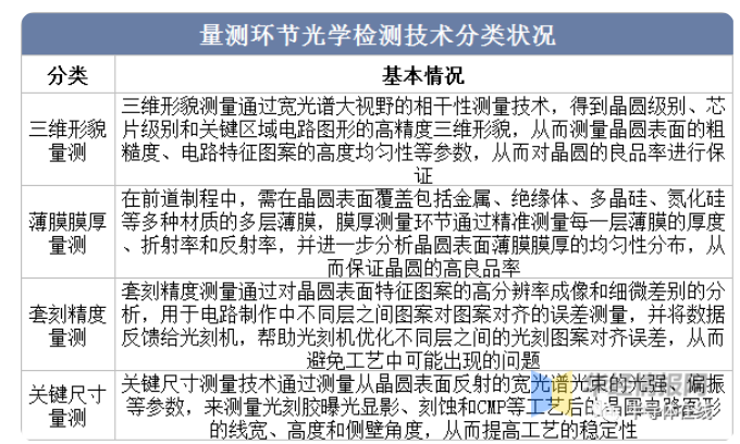
Classification status of optical testing technology in the measurement phase, Source: Public data compilation
3. Global Status of Testing and Measurement Equipment
1. Market Size
In terms of the global semiconductor testing and measurement equipment market size, with the recovery of demand in downstream consumer electronics and PCs from 2020 to 2021, especially a significant increase in 2021, the global market for testing and measurement equipment continues to expand. According to data, the global market size for semiconductor testing and measurement equipment was $7.65 billion in 2020, with a CAGR of 12.6% from 2016 to 2020. The overall semiconductor industry saw a significant increase in 2021, and it is estimated that the scale of testing and measurement equipment has improved significantly.
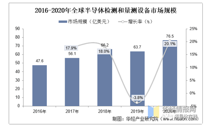
Global semiconductor testing and measurement equipment market size and growth rate from 2016 to 2020, Source: ZK Fei Ce Prospectus, Huajing Industry Research Institute
2. Submarket
The measurement equipment has many subcategories. According to data, in 2020, the market share of various types of semiconductor testing and measurement equipment included defect detection equipment for non-patterned wafers, defect detection equipment for patterned wafers (which can be subdivided into micron and nanometer levels), and mask detection equipment; measurement equipment included three-dimensional morphology measurement equipment, film thickness measurement equipment (wafer dielectric film measurement equipment), overlay accuracy measurement equipment, critical dimension measurement equipment, and mask measurement equipment.
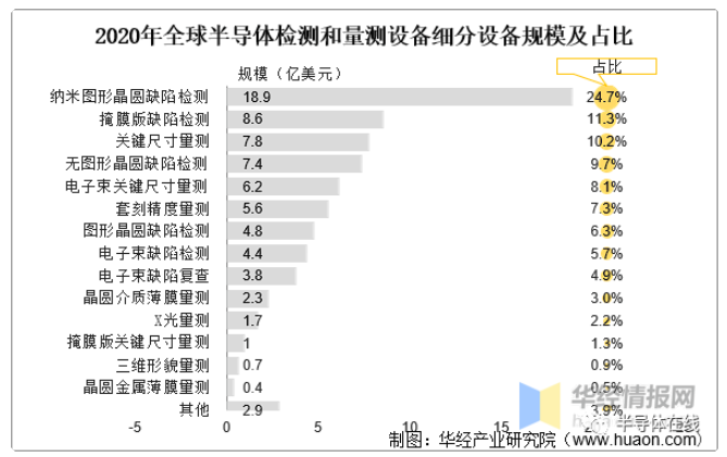
Global semiconductor testing and measurement equipment subcategory size and share in 2020, Source: ZK Fei Ce Prospectus, Huajing Industry Research Institute
3. Technical Structure
Measurement equipment is divided into optical and electron beam technology routes, with optical being the mainstream. In the global semiconductor testing and measurement equipment market in 2020, the shares of optical and electron beam technologies were 75.2% and 18.7%, respectively. Due to the downstream manufacturers’ demand for high-speed mass production, optical testing technology equipment still occupies a major market share.
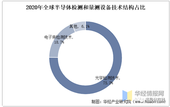
Global semiconductor testing and measurement equipment technology structure share in 2020, Source: ZK Fei Ce Prospectus, Huajing Industry Research Institute
4. Status of Testing and Measurement Equipment in China
Regarding the current status of domestic testing and measurement equipment, the overall semiconductor testing and measurement equipment market in China accounts for about 25% of the global market and continues to show an upward trend. Data shows that in 2021, the scale of testing and measurement equipment in China was $2.9 billion, a year-on-year increase of 61.1% compared to 2020, with a growth rate far exceeding the global scale. However, the domestic market is still mainly occupied by international companies, and the compatibility between technology and enterprises needs to be improved.
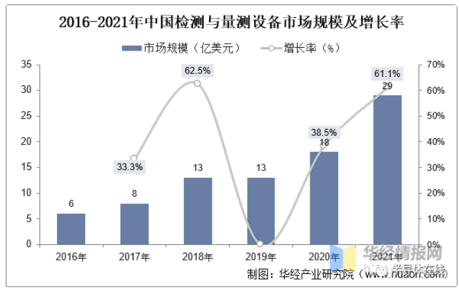
China’s testing and measurement equipment market size and growth rate from 2016 to 2021, Source: Public data compilation
5. Competitive Landscape of Testing and Measurement Equipment
1. Competitive Landscape
The global semiconductor testing and measurement equipment market shows a monopoly pattern dominated by foreign equipment giants. According to data, in the global market, KLA Semiconductor’s market share exceeded 50% in 2020, with the top five companies, including Applied Materials, Hitachi, Reticle Technology, and Innovate Technology, collectively accounting for over 82.4% of the market share, indicating a high market concentration. In the Chinese market, KLA Semiconductor reached 58.4%, showing a dominant position, with the top five companies collectively accounting for 78.1% of the market share.
Local companies have a low market share, among which ZK Fei Ce’s products mainly include non-patterned wafer defect detection equipment, patterned wafer defect detection equipment, three-dimensional morphology measurement equipment, and film thickness measurement equipment, which have been applied in domestic integrated circuit manufacturing lines for processes of 28nm and above. Shanghai Ruile focuses on the research and production of equipment for the front-end process detection in integrated circuit production, with products mainly including optical film thickness measurement equipment and optical defect detection equipment, as well as silicon wafer thickness and warpage measurement equipment. Shanghai Jingce Semiconductor has developed products suitable for semiconductor industrial applications based on elliptical polarization technology for film thickness measurement and optical critical dimension measurement systems. Currently, in 2021, ZK Fei Ce, Jingce Electronics, and Shanghai Ruile only accounted for 1.9%, 0.7%, and 0.2% of the domestic testing and measurement equipment market, respectively.
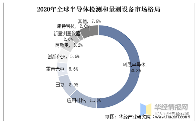
Global semiconductor testing and measurement equipment market structure in 2020, Source: ZK Fei Ce Prospectus, Huajing Industry Research Institute
2. Major Companies
KLA Instruments and Tencor Instruments were established in 1976 and 1977, respectively, and merged in 1997 to form KLA Semiconductor, headquartered in Silicon Valley, USA. The company focuses on the research, production, and sales of testing equipment, with a product line covering the entire range of quality control equipment. According to KLA Semiconductor’s 2022 annual report, its testing and measurement equipment achieved revenue of $7.925 billion, accounting for about 86% of the company’s total revenue.
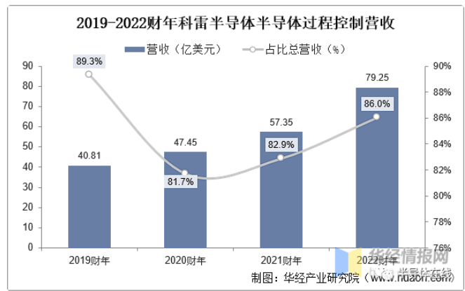
KLA Semiconductor’s semiconductor process control revenue from FY2019 to FY2022, Source: Company Bulletin, Huajing Industry Research Institute
Contemporary Amperex Technology Co., Ltd. was established in 1987 and is headquartered in Migdal HaEmek, Israel. The company is a manufacturer of high-end testing and measurement equipment in the semiconductor industry, with its products applied in front-end, advanced packaging, and other fields, serving many leading global IDM, OSAT, and foundries. According to Contemporary Amperex’s 2021 annual report, it achieved total revenue of $270 million, with testing and measurement equipment revenue of $259 million, accounting for 96.2%.
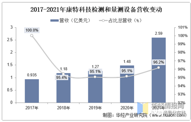
Changes in revenue from testing and measurement equipment of Contemporary Amperex from 2017 to 2021, Source: Company Bulletin, Huajing Industry Research Institute
ASML (Netherlands) has advantages in overlay error measurement and electron beam testing, while Applied Materials (USA) also excels in electron beam testing. Nova Measuring Instruments (Israel) specializes in film thickness measurement equipment, Hitachi (Japan) is a leader in CD-SEM (Critical Dimension Measurement – Electron Beam), and Reticle Technology (Japan) focuses on EUV mask detection, while Innovate Technology (USA) excels in critical dimension measurement and defect detection.
6. Development Trends
1. Technological Trends
As the physical dimensions of integrated circuit devices shrink and gradually develop towards three-dimensional structures, the scales of defects to be detected and the physical scales to be measured are continuously decreasing, while three-dimensional spatial detection is continuously penetrating. To meet the development trends and requirements for high speed, high sensitivity, high accuracy, high repeatability, and high cost-effectiveness in testing and measurement technology, many technical improvements have been made in the industry, such as enhancing the intensity of illumination, extending the spectral range to the DUV band, improving the numerical aperture of optical systems, increasing the optical modes for illumination and collection, and expanding the application of optical algorithms and optical simulations in testing and measurement fields. In the future, as integrated circuit manufacturing technology continues to improve, the corresponding levels of testing and measurement technology will also continue to rise.
2. Localization Trends
There are significant barriers in the overall semiconductor equipment field, including high technology, funding, and industrial collaboration. Compared to foreign companies, local enterprises have entered this field later, and there is a considerable gap in overall strength and scale compared to foreign competitors. However, after years of relentless pursuit, local companies have rapidly improved their technological levels, and testing and measurement equipment has developed from non-existence to existence. Domestic companies like ZK Fei Ce have continuously made breakthroughs in the localization of measurement equipment, currently achieving breakthroughs at 28nm and pushing towards nodes below 2Xnm.
Source | Today’s Semiconductor

 ☞ Business Cooperation: ☏ Please call 010-82306118 / ✐ Or email [email protected]
Click
here to “read the original text”, directly to Electronic Technology Application Official Website