
FPGA is a “reconfigurable logic” device. Chips are manufactured first, then “reconfigured” during redesign.
ASICs do not require “reconfiguration”. You design it first, hand it over to the foundry, and then manufacture the chip.
Now let’s take a look at the structure of these chips and how they differ.
● Logic Units: The Basic Module of FPGA
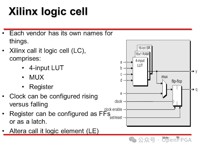
This is the smallest logic block. LUT acts as combinational logic. With the help of DFF, it can form sequential logic.
It can construct logic gates, multiplexers, encoders, adders; any truth table can be stored as a Boolean expression in the LUT.
A LUT can save a limited amount of data. The LUT of a logic unit is also limited.
Boolean expressions with many terms require more memory space, and tools will place remaining terms into another logic unit during layout routing. This requires routing signals between two logic units.
● FPGA Routing Signals
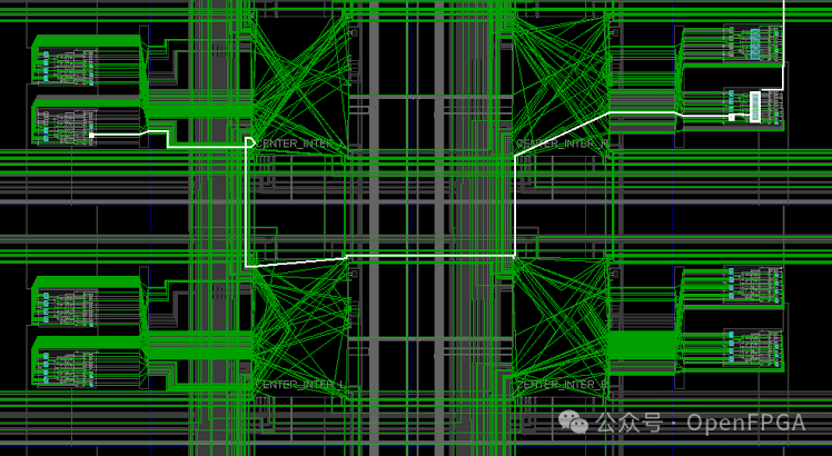
The white lines are signals routed from one logic unit to another. You can imagine how much longer this wire length increases when implementing larger logic. This adds extra delay, reduces clock frequency, and consumes more area and power.
All of this is just for “reconfiguration”.
Even if the design does not require additional units or routing signals, they still exist in the FPGA chip routing area and static power, thus reducing efficiency.
● Standard Cells: The Building Blocks of ASIC
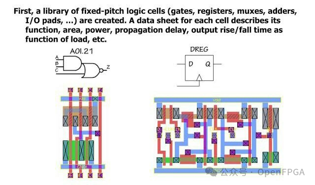
The standard cell library can have components as small as NAND gates and IPs such as adders, FFs, BRAMs, multiplexers, etc.
All standard cell libraries are optimized for area and power.
● ASIC Layout:
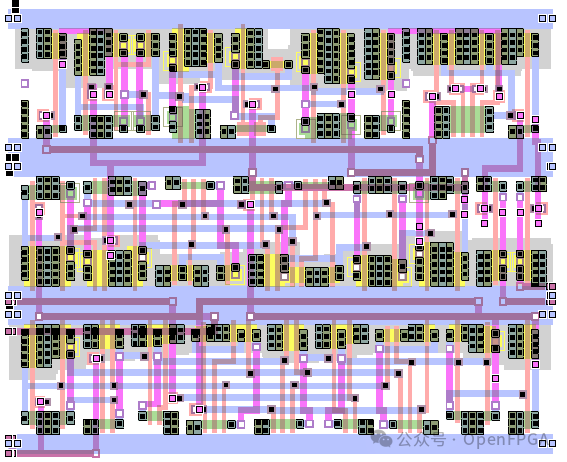
Individual cells are tightly connected to each other, forming larger logical functions. The positions are also optimized for signal propagation. Unlike FPGAs, ASICs do not have unnecessary logic and routing overhead. This saves area and power, and can achieve faster clock speeds.
All of the above means that ASICs are more efficient than FPGAs.
From November 18 to November 29, E Course Network launched the “Advanced FinFET Layout Design Online Live Class”, taught by experienced expert instructors in real-time, in just 2 weeks, it can help students master the analog layout design capabilities under 12nm FinFET technology, and after completing the course, you can choose from quality offers, your next job with a 30% salary increase is not a dream! A must-learn for working analog layout design engineers!
As an analog layout engineer, learning and applying advanced FinFET process knowledge is essential for skill accumulation! Let’s keep pace with technological development, continue learning, and refuse to be eliminated!
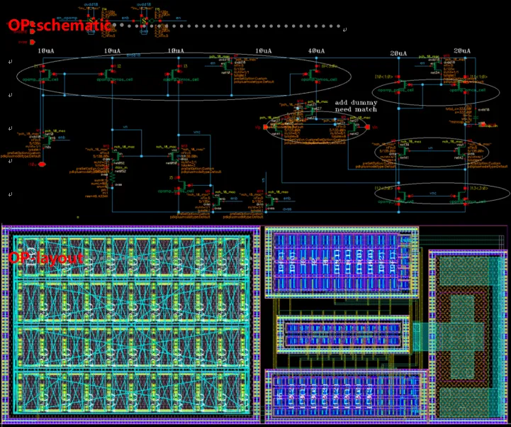
The circuits and layouts of OP used in the course based on FinFET technology
►►►
Target Audience for the Course
2. Working analog layout design engineers
►►►
Course Highlights
2. The course includes 3 projects that progress from simple to complex, using advanced FinFET technology, suitable for students with some project experience who want to learn and practice advanced FinFET process analog layout design.
3. Small class instruction, every night live teaching, FinFET instructors (senior engineers) provide online real-time guidance to help each student accumulate practical project experience and enhance their personal professional competitiveness.
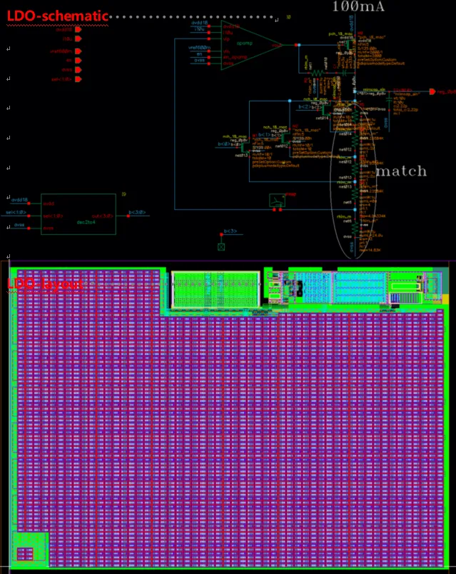
The circuits and layouts of LDO used in the course based on FinFET technology
►►►
Course Objectives
-
Based on advanced FinFET technology, train analog layout engineers with advanced design capabilities through a project-driven approach.
-
Based on achieving tape-out standards, complete the analog layout design work for 3 projects based on FinFET technology.
-
Not just listening to lectures and learning theory, but mastering FinFET layout design methods and process rules to enhance layout design efficiency.
-
Not just mastering basic knowledge, but also delivering quality work according to industry engineering project standards to enhance engineering thinking skills.
-
Not just completing simple experiments, but also independently completing FinFET analog integrated circuit layout designs, accumulating real-world advanced process project experience.
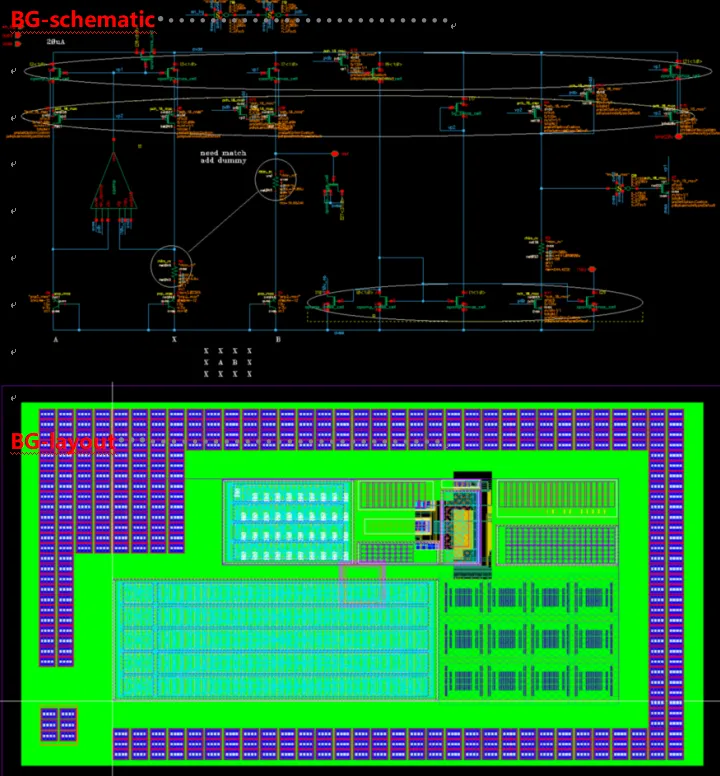
The circuits and layouts of BG used in the course based on FinFET technology
►►►
Course Outline
| Learning Stage | Course Theme | Course Content |
| Stage One | Fundamental Knowledge of FinFET Technology and Process Document Rules (layout notice) | Advanced FinFET Process▪ Basic knowledge of advanced FinFET technology▪ Advanced FinFET process library files PDK, rule files▪ Important considerations for advanced FinFET analog layout design |
| Stage Two | Project Environment Establishment and Tool Utilization | New Tools for Analog Layout▪ New analog layout tools▪ Verification process, main differences between FinFET devices and regular processes |
| Stage Three | FinFET Layout Projects | Layout Projects Based on FinFET Technology▪ Logic gate design (Dec2to4), OP, BG, LDO▪ Dec2to4 layout design▪ Practical layout design of OP using advanced FinFET technology▪ Practical layout design of BG using advanced FinFET technology▪ Practical layout design of LDO using advanced FinFET technology |
| Stage Four | Online Practical Problem Solving and Experience Summary Exchange | Problem-solving and summarizing DRC, LVS, EMIR, etc., during FinFET process layout projects to enhance project experience▪ Provide real FinFET projects and practical environments, complete three projects▪ How to upgrade from regular processes to advanced FinFET processes▪ Master physical verification of analog layout under advanced FinFET technology, summarize experiences |
►►►
Instructor Introduction
Over 6 years of experience in analog layout design, multiple tape-out experiences, and rich project delivery and management experience. Familiar with process nodes such as 180nm, 40nm, 28nm, and 12nm. Won the second prize in the 2021 National Industrial and Information Technology Skills Competition for the employee group.
Head of the E Course Network analog layout design course, deeply engaged in various analog layout chip design projects with rich teaching experience, holding a qualification certificate for integrated circuit engineering technical personnel training.
►►►
Course Start Time
Course Start Time
Class Schedule
The course includes a 3-month VNC server, allowing students to practice 24/7
►►►
Learning Methods
►►►
Course Fees
Promotional limited-time special price, register for only6980 yuan
The first 5 people can receive a 1000 yuan coupon After the coupon5980 yuan
p.s. The course video (live replay) is valid for 365 days, and the VNC server is valid for 3 months
►►►
Registration Consultation
Individuals and companies interested, please contact E Course Network teachers via WeChat for consultation and registration!

Scan to add E Course Network teachers on WeChat


E Course Network (www.eecourse.com) is a professional integrated circuit education platform under Moore Elite, dedicated to cultivating high-quality integrated circuit professionals in the semiconductor industry. The platform is oriented towards the job requirements of integrated circuit companies, providing training platforms that fit the corporate environment, and quickly training students to meet corporate needs.
The E Course Network has a mature training platform, a complete course system, and strong faculty resources, planning a total of 168 high-quality semiconductor courses covering the entire integrated circuit industry chain, and has 6 offline training bases. So far, a total of 15,367 people have been deeply trained, directly supplying 4,476 professional talents to the industry. Established deep cooperative relationships with 143 universities and held 240 corporate-specific IC training sessions.