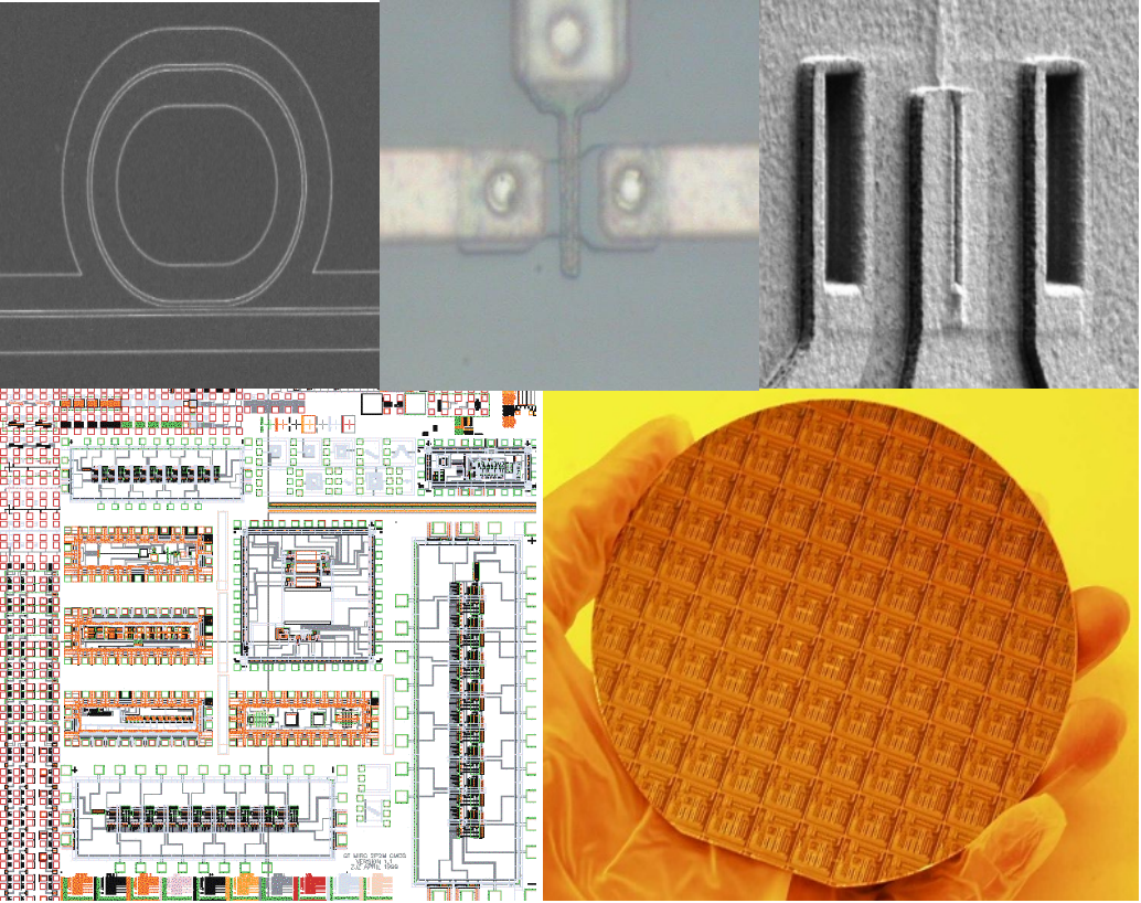
 Silicon-based optoelectronic chips represent the highest stage of semiconductor chip development. This image is provided by the author.
● ● ●
Chips are a topic that is both familiar and unfamiliar. Each of us has heard of chips and interacts with them daily. Especially recently, apart from research institutions, government agencies, and the capital market taking it seriously, people are discussing chips in stores, on trains, in butcher shops, and cement factories, with some even planning to start chip manufacturing businesses. However, the vast majority of people have never truly seen what a chip looks like, let alone understand how they work and differentiate between different chips.
Over 60 years ago, people began processing chips on silicon wafers. The chips of that time were very simple, some with only one transistor, but they already demonstrated tremendous advantages over vacuum tubes in terms of size, energy consumption, and price. That era is known as the transistor era.
Then came the familiar integrated circuit era, followed by the optoelectronic era, and now we are in the less familiar silicon-based optoelectronic era. These different eras have actually evolved with the development of semiconductor chips.
Just as the main function of the human heart is to propel blood flow and provide sufficient blood supply to other organs and tissues to maintain their normal metabolism and function, in today’s information society, semiconductor chips are responsible for processing information and transmitting it to every corner of various industries. The strength of chip functionality determines the strength of the information society. The ‘chip’ pain caused by the lack of core chips could lead to stagnation or even extinction of the information society.
To truly understand chips, the first step is to clarify the following four basic concepts: What are electrons? What are photons? What is the spectrum? What are semiconductors? These terms may sound very esoteric, but they are actually quite understandable.
Electrons and photons are fundamental particles that make up matter. A large number of electrons form current, transmitted through metal wires; a large number of photons form light beams, propagated through optical waveguides. The difference is that electrons can interact with each other: two currents intersecting will form a short circuit and merge into one; the interaction between photons is not so straightforward: two beams of light crossing still travel their own paths.
The spectrum is the characteristic of photons, expressing the different frequency distribution of photons. It can carry different information. Therefore, a single wire can only transmit one signal; while in an optical waveguide, many different signals can be transmitted simultaneously, greatly increasing communication capacity and speed.
Semiconductors refer to materials that have electrical conductivity between conductors and insulators at room temperature. Common semiconductors include silicon, germanium, gallium arsenide, indium phosphide, etc. Silicon is the most successful semiconductor in commercial applications.
In semiconductor crystals, specific impurity elements are artificially doped to control their conductivity, making semiconductors the best material for manufacturing electronic chips.
In semiconductors, electrons and photons have strong interactions: applying electricity can produce light; light can generate electricity. They are the foundation of optoelectronic chips.
So far, four different types of chips have developed on semiconductor materials, which can also be called semiconductor chips. They rely on electrons, photons, or optoelectronic interactions, which determine their characteristics and uses.
Since J.J. Thomson confirmed the existence of electrons in 1897, electrons have experienced the vacuum tube era (1905), the transistor era (1947), and reached the integrated circuit era (1958). The so-called integrated circuit is a type of electronic chip, which we all hear about and use every day, known as IC chips. Integrated circuits primarily use silicon as material, with one important feature being that they only utilize electrons as information carriers.
With the push of Moore’s Law and the efforts of chip companies and instrument manufacturers, the electronics industry has now become an inseparable part of the global economy.
The term photon was only recognized in 1927. After experiencing the spatial optics era and the integrated optics era, experts and scholars, borrowing from the path of electronic development, used similar technologies and methods to integrate large optical components onto a small substrate, forming the photon chip. The important feature of photon chips is that they only use photons as information carriers, without the participation of electrons.
Due to the very weak interactions between photons, it is impossible to form low-cost, low-energy functional devices, and the industrial scale is virtually non-existent. Therefore, the current research focus of photon chips is primarily on basic research rather than industrial development.
Both of the aforementioned chips have serious limitations. For example, electronic chips have a main frequency limited to a few GHz due to the restrictions of the speed of electrons moving within semiconductors. Photon chips, due to the weak interactions of photons, are essentially passive devices with very limited functionality.
To solve the above problems, people naturally thought of combining photons and electrons. In fact, it was during the study of photons that researchers found their inseparable relationship with electrons: semiconductor materials can generate electrons by absorbing photons and can emit photons through the annihilation of electrons. This opened the research into optoelectronics and led to the invention of lasers and photodetectors—the simplest optoelectronic chips. The era of optoelectronic chips began in the 1970s. To achieve a stronger photoelectric effect, early optoelectronic chips were primarily made from gallium arsenide and indium phosphide materials. However, these materials are difficult to process and hard to create in sizes as large as single-crystal silicon. Thus, the optoelectronic chips made from them are costly, and due to low integration, their functionality is very limited.
The emergence of optoelectronic chips provided a rapid development opportunity for the communication industry, particularly in optical communications. With the advent of high-performance lasers, erbium-doped fiber amplifiers, and wavelength division multiplexers, communication systems have transitioned from cable transmission to fiber optic transmission, evolving from single-line single-path to single-line multi-path, significantly enhancing transmission rates and throughput while reducing costs, allowing many households to enjoy the benefits of fiber-to-the-home, laying the foundation for the upcoming big data era.
From the introduction of the above three types of chips, it can be observed that due to the inherent characteristics of electrons and photons, their development in industrial applications is entirely different.
Electrons have strong interactions, thus forming the ‘electronic industry’; photons, having virtually no interactions, cannot form their own industry.
Currently, products related to photons, aside from optical waveguides, are primarily the result of the combined action of optoelectronics. The ‘optoelectronic industry’ has already widely entered the consumer market.
The ‘photon industry’ is merely a concept and cannot enter the consumer market unless the ‘optoelectronic industry’ is renamed the ‘photon industry’.
Looking at the history of semiconductor chip development, electronic chips/integrated circuits, photon chips, and optoelectronic chips are merely special stages within it. The current trend in semiconductor chip development is to organically unify and integrate them onto a silicon substrate, forming a brand new silicon-based optoelectronic chip.
As is well known, the guiding ‘Moore’s Law’ for microelectronics has basically failed, and the development of integrated circuit chips is nearing saturation. On the other hand, due to the development of big data, cloud computing, and the Internet of Things, the data flow on various branch lines of the information highway system has greatly increased. To enhance chip speed, scientists in developed countries and regions such as the United States proposed the concept of optical interconnects in the mid-1990s, extending ‘optics replacing copper’ into the interior of chips. They used technologies and methods compatible with silicon-based integrated circuit technology to integrate micro-nano-level photonic, electronic, and optoelectronic devices on the same silicon substrate, forming silicon-based optoelectronic chips.
In simpler terms, to meet the growing demand for data flow, while electronic chips are unable to cope, photons are added to the current silicon-based integrated circuits to form a new type of large-scale optoelectronic integrated chip that is both fast and cost-effective.
Many large companies such as IBM, Intel, TSMC, GlobalFoundries, Cisco, and Acacia have already begun commercial mass production of silicon-based optoelectronic chips, and optical modules centered around silicon-based optoelectronic chips have also gained extensive applications in data centers and communication systems, forming a silicon-based optoelectronic industry chain.
Silicon-based optoelectronic chips can bring significant advantages in computing power, energy consumption, cost, and size. It is anticipated that they can support communication devices, data centers, supercomputing, IoT sensors, artificial intelligence, and other industries in the big data era, and may soon enter the consumer market.
People’s understanding of electrons and photons, and the resulting technological eras, has led to the emergence and development of the information society. The information society’s preference for compact, inexpensive, and low-energy devices and systems has spawned various types of semiconductor chips.
The earliest electronic chips, or rather, integrated circuits, benefited from the perfect combination of silicon materials and CMOS devices, featuring small size, low cost, and high integration, and have now become an inseparable part of the global economy, evolving into a traditional industry with a development speed that has saturated and slowed.
Photon chips utilize photons as information carriers. Due to the very weak interactions between photons, it is impossible to form low-cost, low-energy functional devices, and thus cannot form their own industry.
Optoelectronic chips focus on the interaction between photons and electrons, characterized by multi-channel, large bandwidth, and high speed, which are key technologies supporting high-speed communication. However, as they are made from gallium arsenide and indium phosphide materials, it is challenging to achieve low cost and high integration.
Silicon-based optoelectronic chips represent the highest stage of semiconductor chip development. They are large-scale optoelectronic integrated chips obtained by heterogeneously integrating the basic elements of the aforementioned three chips onto a silicon substrate. They are recognized as core technologies in the post-Moore’s Law era and the cornerstone of the big data era.
As a part of the universe, chips also follow natural laws, forming and developing in stages and progressively. Specifically, chips are a convergence of human intelligence and essence, an artistic creation resulting from long-term research and development in cutting-edge science and technology, not a low-barrier product that can be quickly obtained with a large amount of money.
Specific stages of chips will play specific roles, each with its advantages and disadvantages.
In today’s information society characterized by big data and artificial intelligence, pure electronic chips/integrated circuits can no longer meet the needs for data transmission and processing, nor can they bring about the next era of transition.
Simply emphasizing the multi-channel transmission characteristics of photons and the concept of photon chips will not only fail to expand the photon industry but may also misdirect efforts to ‘strengthen national strategic scientific and technological capabilities’.
Disregarding the foundation of electronic chips and neglecting the interaction between photons and electrons while treating silicon-based optoelectronic chips as photon chips for study is akin to building castles in the air; without certain conditions for electronic chip manufacturing and industrial accumulation, it is also impossible to produce advanced silicon-based optoelectronic chips.
Silicon-based optoelectronic chips are built on the foundation of electronic chips. They can not only replace some high-end integrated circuits but also open up new application areas, forming a silicon-based optoelectronic industry that is larger than the integrated circuit industry.
Only by truly understanding chips, the development processes of chips, and the different stages of chip development, from foundational innovation and talent cultivation to industrial layout, can we respect the natural laws of chip development and rely on solid cultivation and appropriate resource allocation to efficiently obtain core chips and no longer experience ‘chip’ pain.
December 22, 2020, at Zhongguanyuan, Beijing
This article is jointly published by Intellectuals and the WeChat public account of China Laser.

Zhou Zhiping, Ph.D. from Qiao Zhi Ya Polytechnic Institute, Professor at Peking University. OSA Fellow, SPIE Fellow, IET Fellow; Honorary Director of the Chinese Optical Society, Executive Director of the Chinese Optical Engineering Society; Founding Editor of Photonics Research. He has personally participated in and witnessed the early development, mid-term efforts, and current ‘chip’ pain of China’s microelectronics industry; has conducted in-depth research on the applications of optoelectronic technology in processing, entertainment, sensing, communication, computing, and artificial intelligence; has published over 600 papers, book chapters, patents, and invited reports on micro-nano optoelectronic integration technology, guiding over a hundred students from China and abroad. He authored the first domestic book on ‘Silicon-based Optoelectronics’, defining it as a new technology for large-scale heterogeneous integration of photons, electrons, and optoelectronic devices on the same silicon chip using silicon-based integrated circuit processes and methods, which unifies photonics, electronics, optoelectronics, and communication technology on a silicon substrate.
Layout Editor | Lucas
1.The Significance of Dirac Notation Integral in Quantum Theory | Fan Hongyi
9.From Einstein’s Curiosity to Quantum Information Technology | High Energy Forum