Introduction
Integration
1
Levels of Integration
Electronic system integration is mainly divided into three levels: integration on the chip, integration within the package, and PCB-level integration, as shown in the figure below:
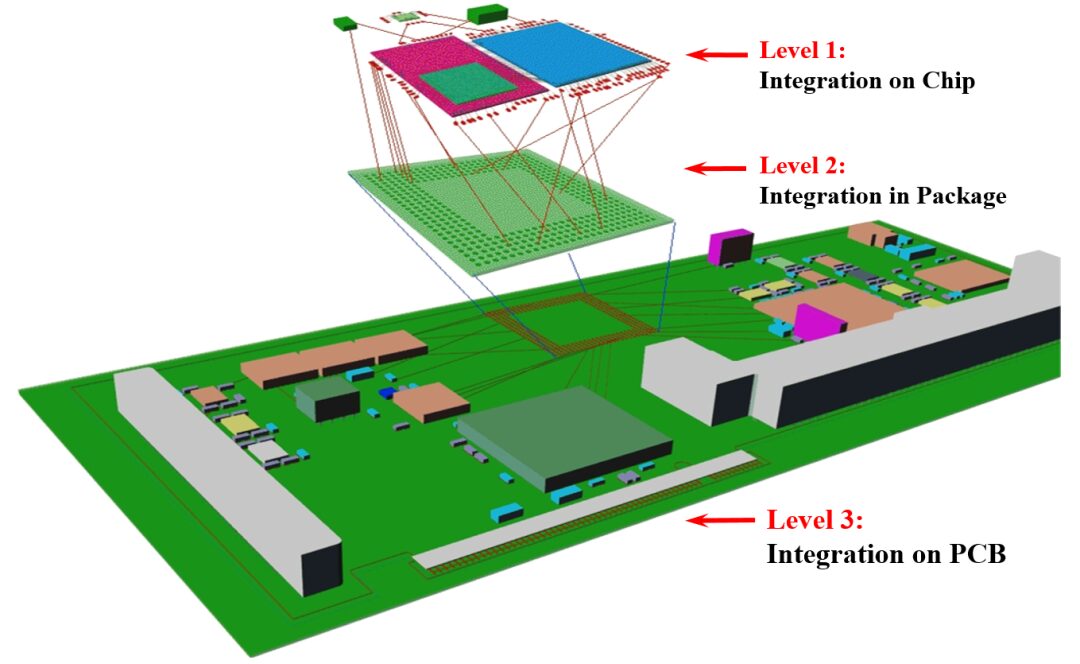
The basic unit of integration on the chip is the transistor, which we refer to as the Function Cell. A large number of Function Cells integrated together form the chip.
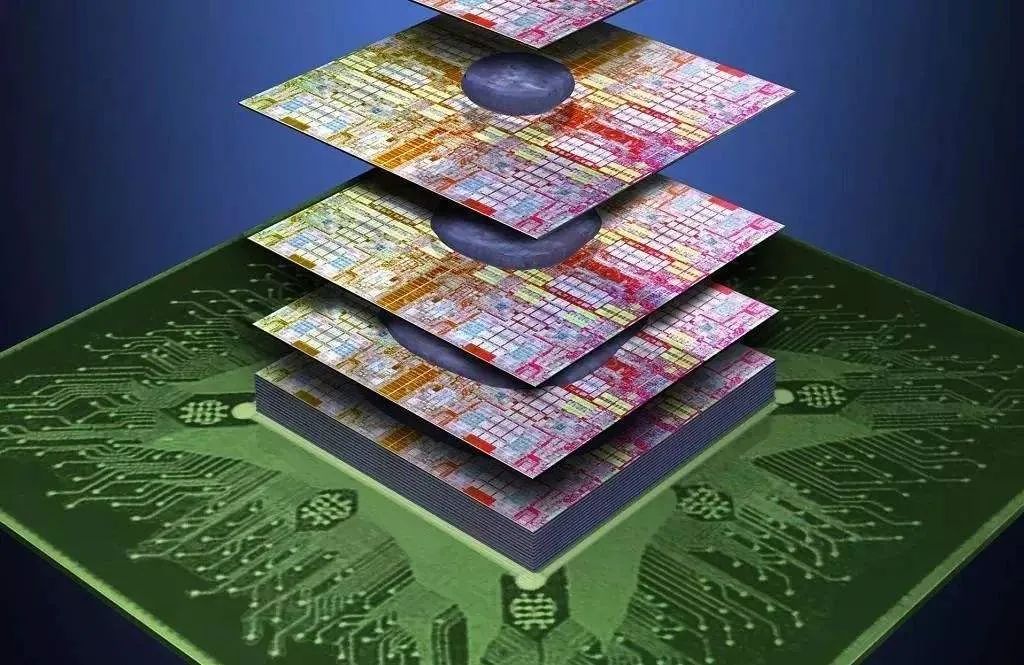
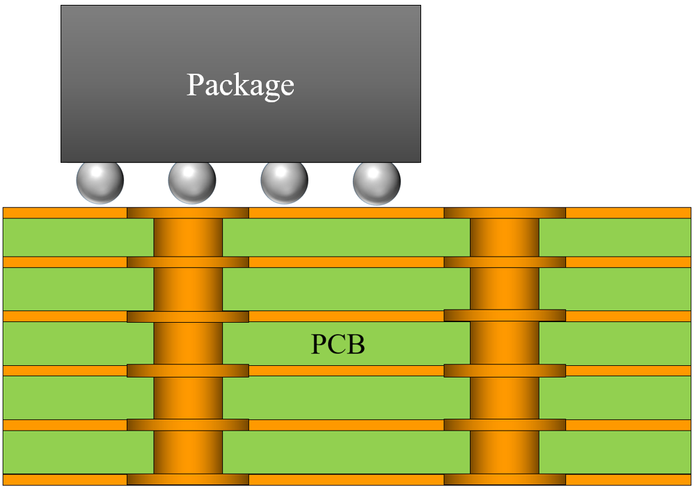
The basic unit of integration within the package is the bare chip or small chiplet completed in the previous step, referred to as the Function Unit. These Function Units are integrated within the package to form a SiP.
The basic unit of integration on the PCB is the package or SiP completed in the previous step, referred to as the MicroSystem. These MicroSystems are integrated on the PCB to form larger-scale systems.
It can be seen that the levels of integration proceed step by step, with each level’s function continuously improving based on the previous level, and the scale constantly expanding.
By the time we reach the PCB level, the electronic system’s functions are already quite complete, and the scale is expanded to a point suitable for human manipulation, along with other components, forming the most commonly used system—Common System, such as the mobile phones or computers we interact with daily.

Integration on the Chip
The transistors on the chip are called Function Cells because they are the smallest indivisible functional units.
The number of Function Cells also serves as an important indicator of the system’s advancement. The human body has approximately 40-60 trillion cells; for a system to be truly intelligent like a human, it may need to contain a similar order of magnitude of Function Cells.
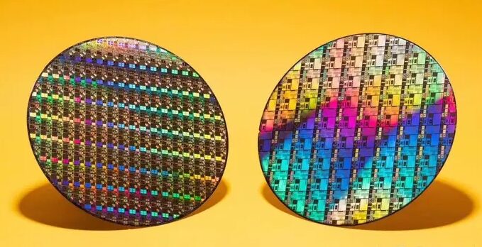
To integrate more Function Cells, transistors can only become smaller and smaller. Today’s transistor sizes may be a billionth of the size of the first transistor invented, while their basic functions remain unchanged.
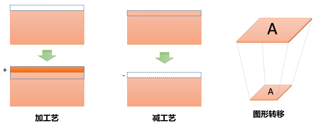
Integration on the chip requires first manufacturing Function Cells and integrating them together. How are these transistors, which serve as Function Cells, manufactured and integrated? From a minimalist perspective, we need to understand three types of materials and three types of processes.
Conductors, Semiconductors, Insulators
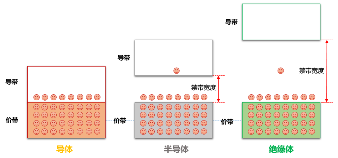
Although there are many materials on the chip, the materials used in modern integrated circuits can almost exhaust the periodic table of elements. All materials can be divided into three categories: conductors, semiconductors, and insulators.
Conductors are responsible for transmitting electrons, insulators are responsible for isolating electrons, and the most important is the semiconductor, as it is variable. It can sometimes act as a conductor (on) allowing electrons to pass through, and sometimes as an insulator (off) blocking electron flow. Furthermore, this change is controllable by designing special structures and applying current or voltage.
In conductors, the conduction band overlaps with the valence band, where there is no forbidden band, making it easy for electrons to move and form current under an external electric field; in semiconductors, a small portion of electrons can jump to the conduction band and form current under an external electric field; in insulators, electrons cannot cross the forbidden band, thus cannot form current.

Integration within the Package
Not all chips or chiplets need to be integrated within the package; a single chip can also be directly packaged and applied on the PCB. However, as Moore’s Law gradually becomes less effective, integration within the package is receiving increasing attention. Concepts such as SiP, advanced packaging, chiplet, heterogeneous integration, 2.5D, and 3D are becoming the focus of the industry, and integration within the package has finally ushered in its spring.

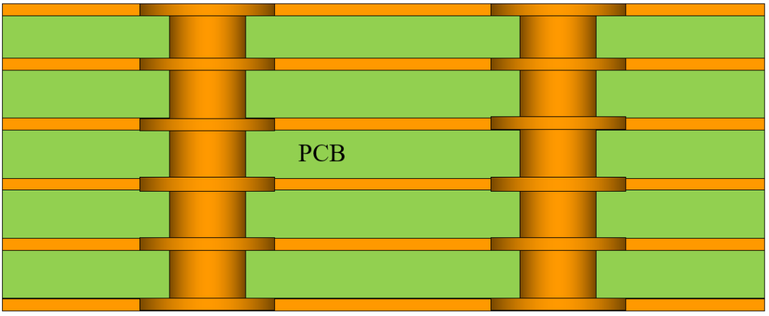
Integration on the PCB
From the history of electronic integration, PCB integration should be the earliest to appear. The emergence of PCBs predates packaging by 11 years and integrated circuits by 22 years.
Before the advent of PCBs, components were directly connected with wires, which not only looked messy but also made it difficult to increase integration density.
Although the PCB has the longest history compared to integrated circuits and packaging, its development in integration technology has been relatively slow due to constraints from packaging size and pin density. It has evolved from single-sided boards to double-sided boards and multilayer boards, with assembly technology evolving from through-hole mounting to surface mount technology (SMT), with assembly density increasing.
Today, PCBs mostly have components mounted on both sides, with layer counts reaching dozens. High-density HDI boards, rigid-flex boards, microwave circuit boards, embedded device boards, etc., are widely used.
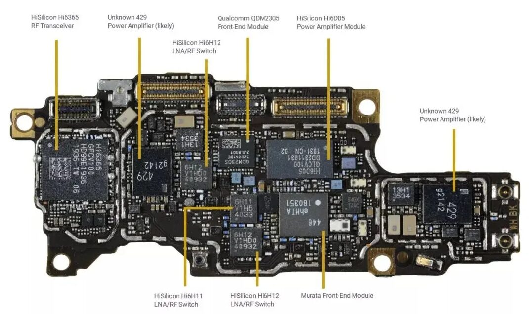
Similar to integration within the package, PCB integration does not utilize the characteristics of semiconductors; thus, the materials used are mainly divided into two categories: conductors and insulators. The main purpose of integration is to electrically connect the MicroSystem modules completed in the previous layer (integration within the package) and, along with other components, form Common Systems, such as the mobile phones and computers we commonly use.
Integration
2
Steps of Integration

Steps of Integration on the Chip
-
Device Manufacturing (Front-end Process)
-
Metal Interconnection (Back-end Process)
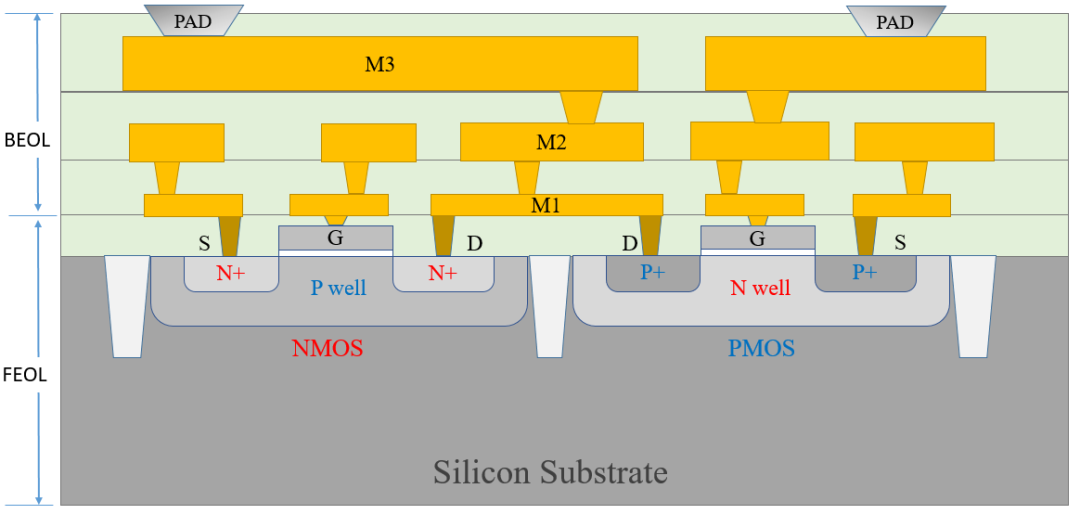
After the transistor layer is manufactured, tungsten or other metals are used to create contact holes connecting the transistors and the first-level wiring, followed by multi-layer metal wiring and vias for electrical interconnection. Earlier chips used aluminum wiring, while modern chips predominantly use copper wiring.
The manufacturing of multi-layer metal wiring used to connect transistors and other components mainly includes dielectric deposition between interconnect lines, metal line formation, and pad formation, generally referred to as the back-end process (BEOL, Back End of Line).
Conductors used in metal interconnection include tungsten, copper, aluminum, etc., while insulators include silicon oxide, silicon nitride, high-k dielectrics, low-k dielectrics, polyimide, etc.
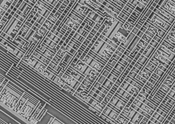
The following image shows a photograph of the metal interconnect lines on a chip under a microscope, illustrating the multi-layer wiring structure, with current processes supporting over 10 layers of metal wiring.
The more advanced the integrated circuit process is, the smaller the structural dimensions become, leading to various effects emerging. To address these effects and manufacture functional transistors, the variety of elements used has increased, almost exhausting the periodic table of elements.
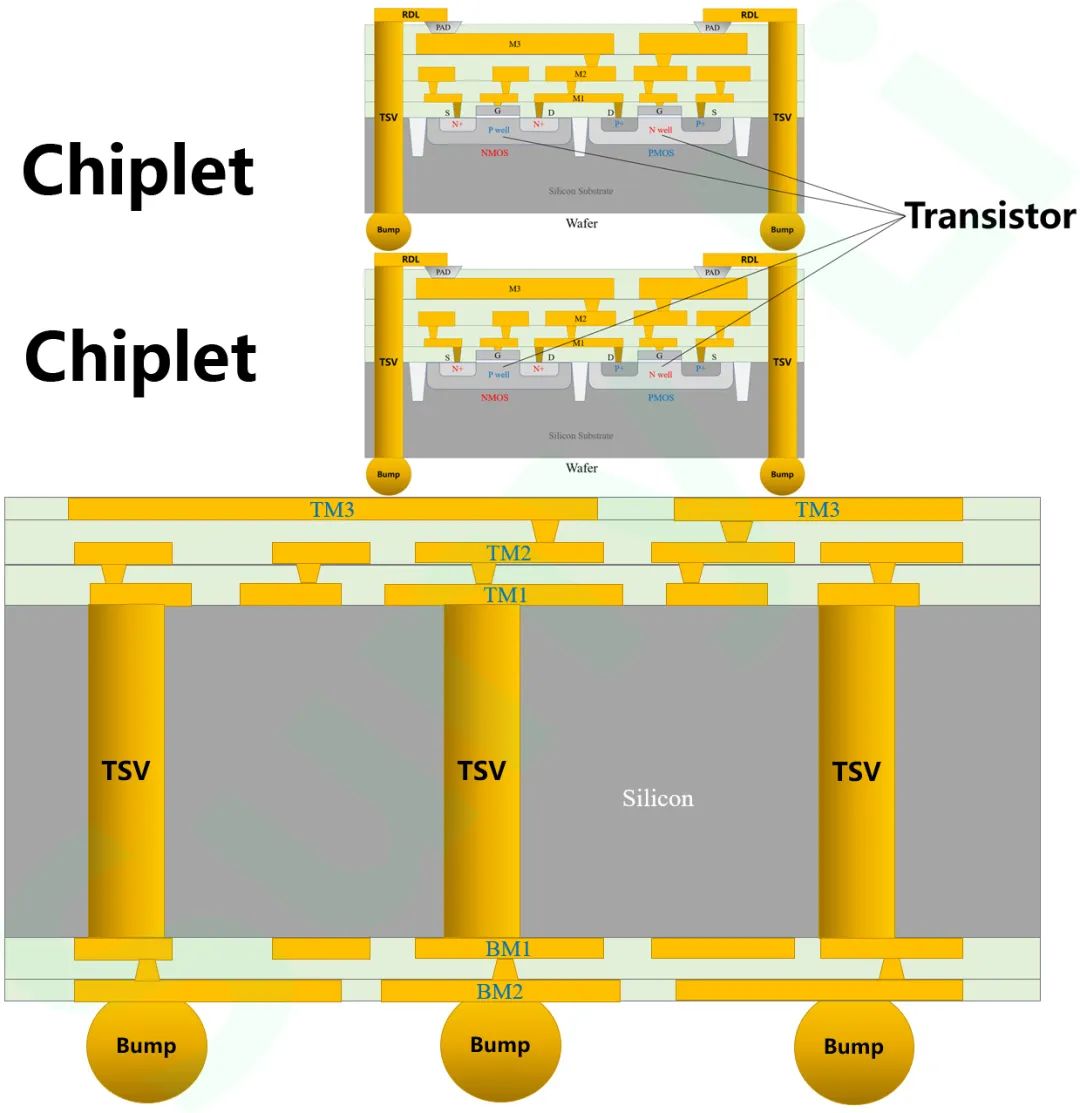
The following diagram illustrates the structural schematic of the front-end process (FEOL) and back-end process (BEOL). First, transistors are manufactured on a silicon substrate, then connected through metal interconnections and brought out to the chip’s PAD.

Steps of Integration within the Package
-
RDL and TSV Production on the Chip
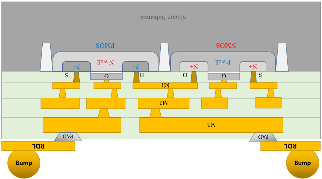
However, the development of TSV technology is becoming increasingly powerful, with claims that up to one million TSVs can be etched in an area of 1mm², fully meeting the needs for high-density interconnections.
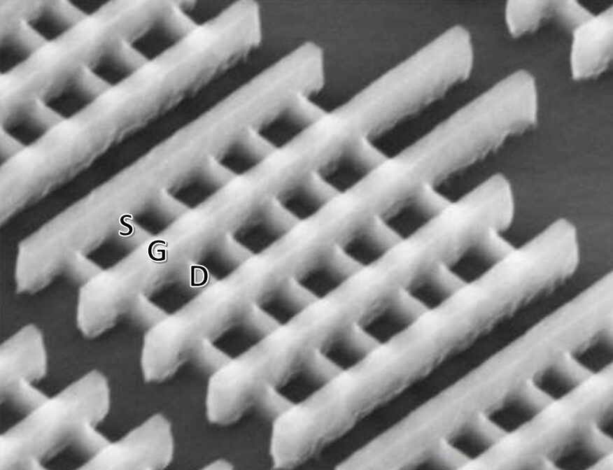
The following image illustrates the schematic of TSV on the chip, which connects the upper and lower surfaces of the chip through metal conductors, preparing for chip stacking.
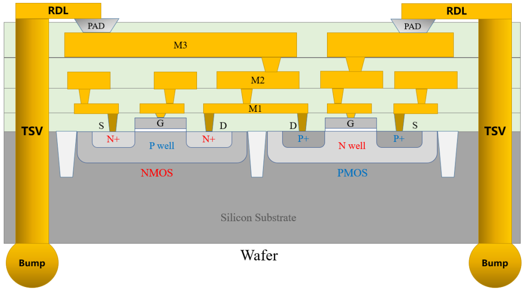
Creating TSV on the chip is extremely challenging, and only leading foundries can accomplish this. This type of TSV is usually referred to as 3D TSV.
To further enhance integration density, people have also invented TSV production on silicon substrates called 2.5D TSV.
-
RDL and TSV Production on the Interposer
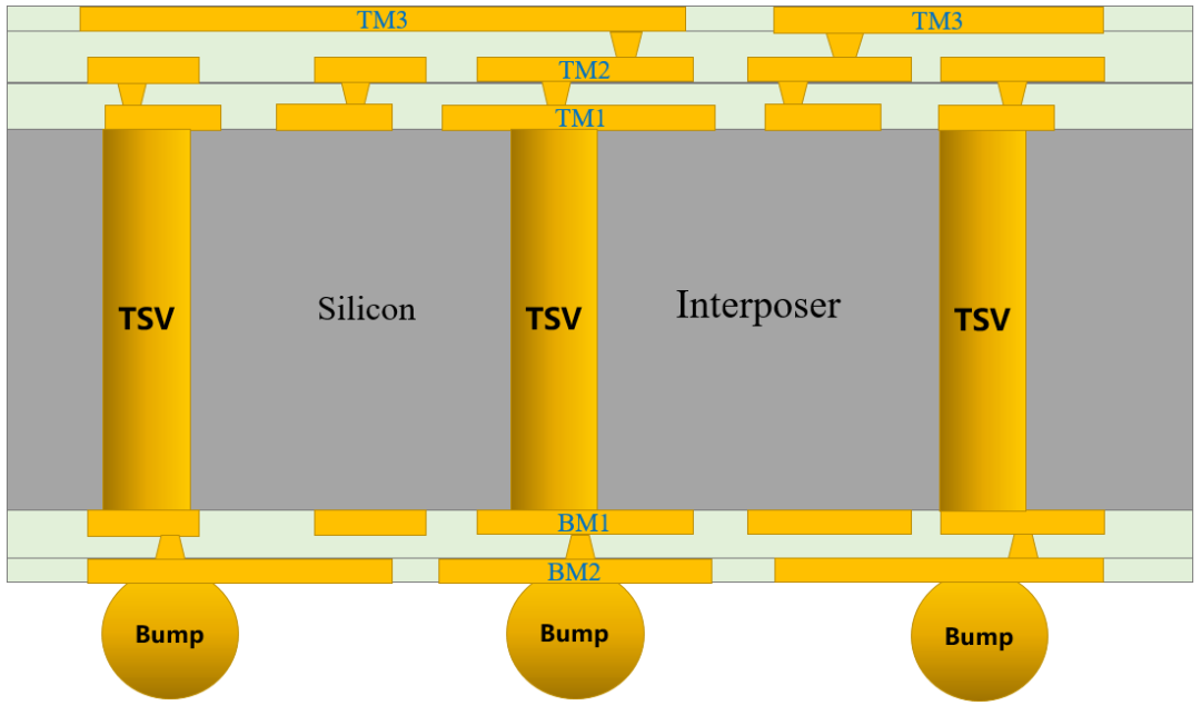
Interposer, known as a silicon interposer, can provide higher interconnection density than ordinary substrates.
The following image shows a typical silicon interposer, with three metal layers on top, two metal layers on the bottom, and connections through silicon vias, which we call a 3+2 structure.
-
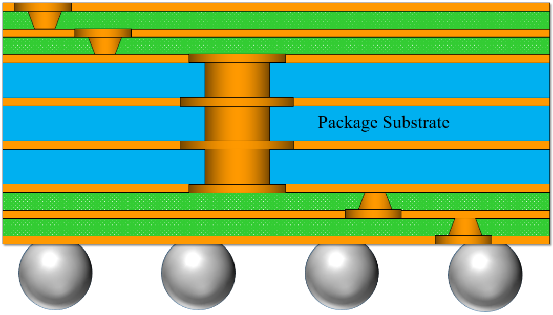
Manufacturing Interconnection Lines on the Substrate
Next, we also need to manufacture the packaging substrate. The materials for packaging substrates vary widely and can be classified into organic substrates and ceramic substrates.
-
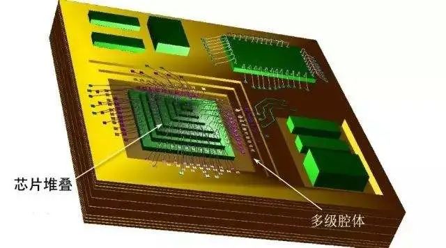
Device Assembly and Packaging
Next, we assemble the chiplets, interposers, and substrates together and apply advanced packaging processes to form a complete advanced package.
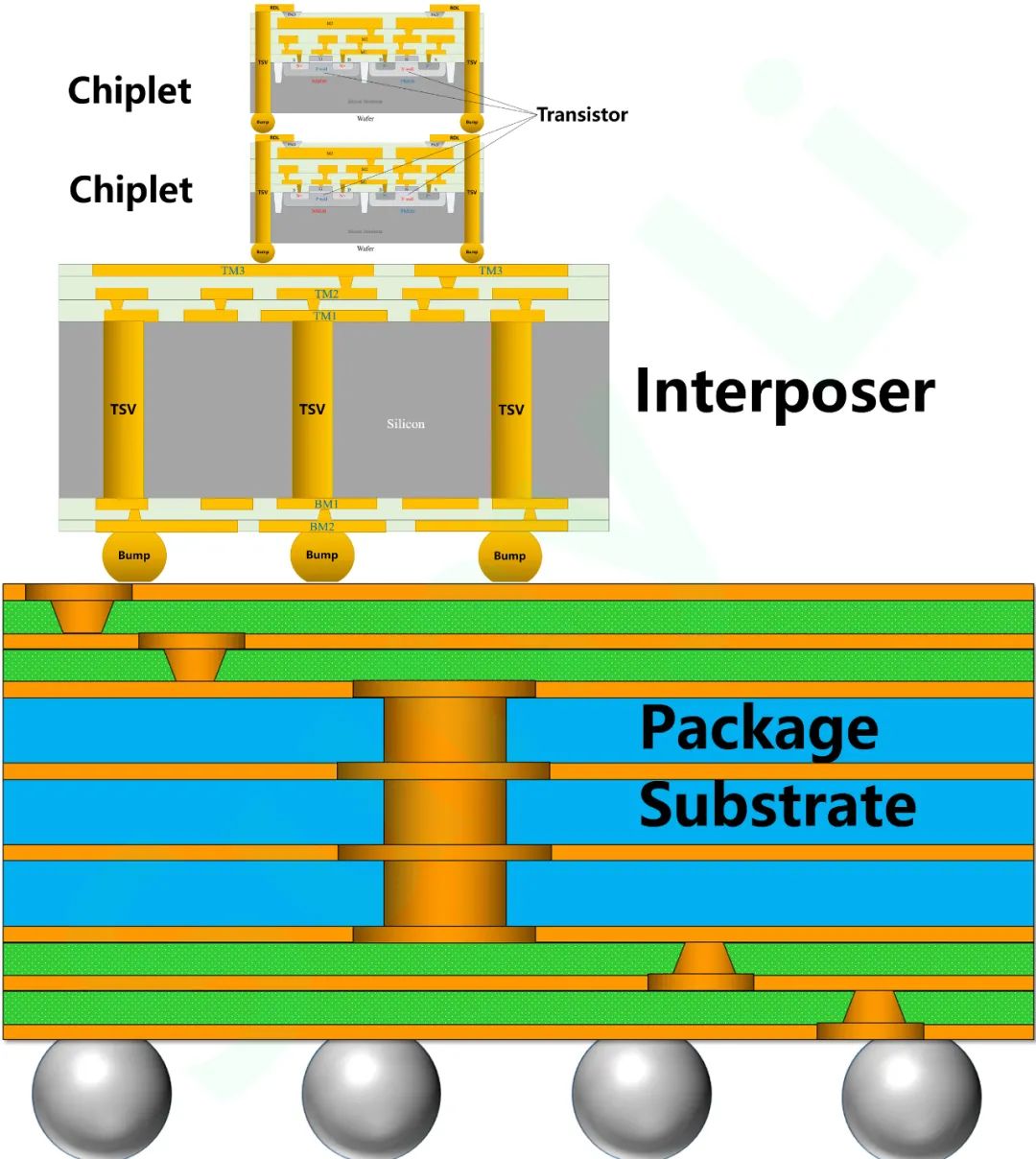
The result of integration within the package possesses the functionality of a system and is compact in size; we can refer to it as SiP or MicroSystem.

Steps of Integration on the PCB
-
Manufacturing PCB Interconnection Lines
-
Component Assembly on the PCB

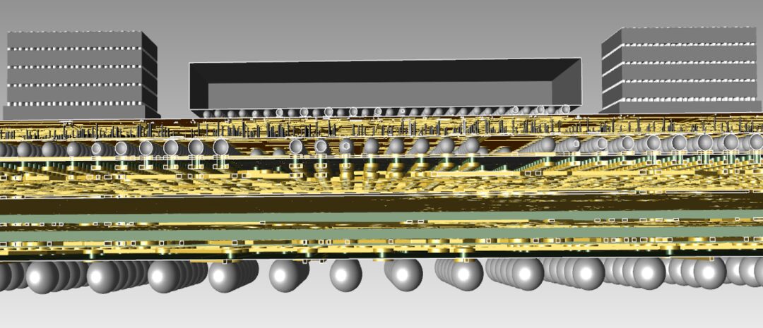
Overall Diagram from Transistor to PCB
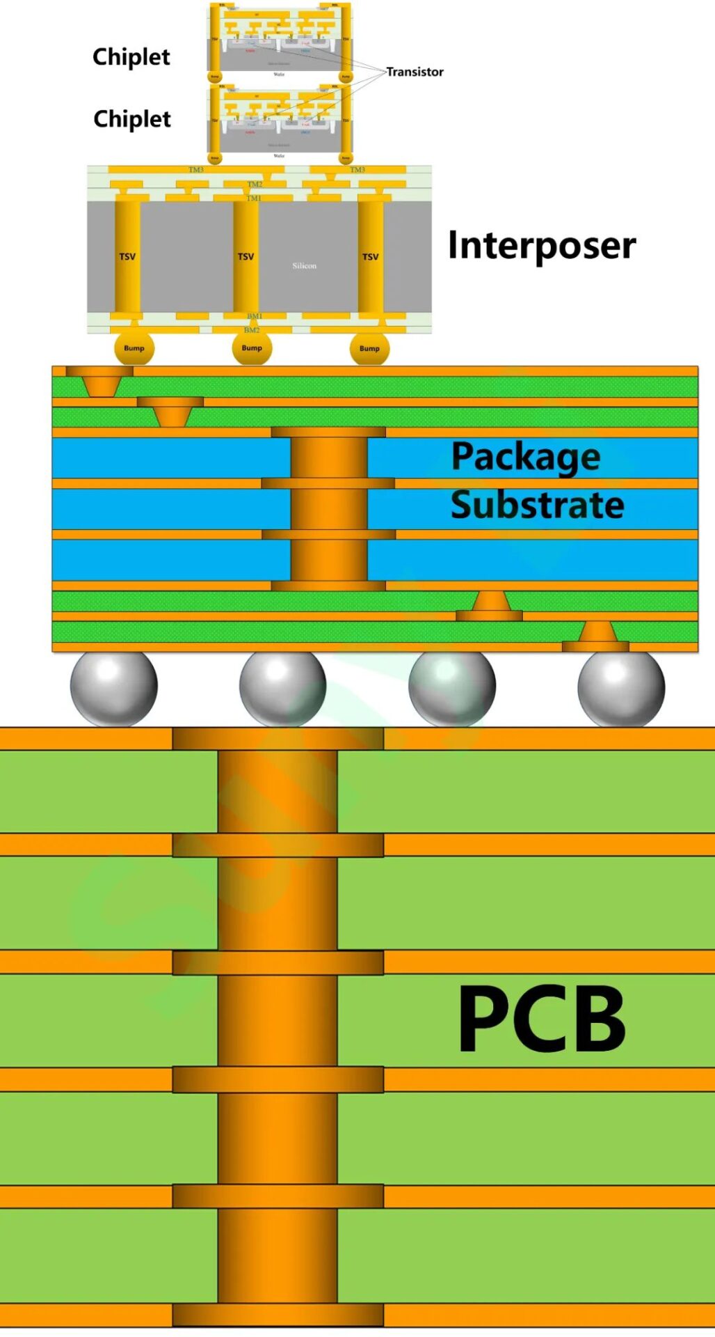
(It is recommended that readers save this diagram, as it may be the first diagram in the industry illustrating the complete integration from transistor to PCB, hand-drawn by Suny Li. As this is a schematic diagram, it is not drawn to scale; in reality, the size expands by about 1,000,000 times from transistor to PCB.)
Editor: Lu Dingci