What is covered?
-
Introduction to SPI Protocol
-
4-Wire or 3-Wire?
-
4 Operating Modes
-
Multiple Transmission Rates
-
Timing of SPI Protocol
-
Upgraded SPI Protocol
-
FPGA Implementation of SPI Protocol
-
Comparison of SPI and IIC
-
Conclusion
Introduction to SPI Protocol
The three most commonly used serial communication protocols between different chips on a board are UART, I2C, SPI. Today, we will introduce SPI Protocol. SPI stands for Serial Peripheral Interface, a high-speed and full-duplex bus protocol developed by Motorola.

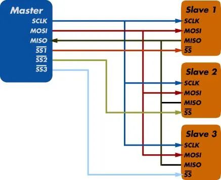
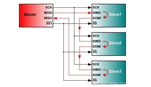
Similar to IIC, SPI also works in a master-slave configuration, where the master is typically an FPGA, MCU, or DSP, and the slave is usually an EPROM, Flash, AD/DA, or audio/video processing chip. It generally consists of four lines: SCLK, CS, MOSI, and MISO. In some cases, they may be referred to as SCK, SS, SDI, SDO, etc., all having the same meaning. When multiple slaves are present, CS is used to select the slave device to control. There is a protocol similar to standard SPI called TI’s SSP protocol, which mainly differs in the timing of the chip select signal.
4-Wire or 3-Wire?
When we talk about SPI, we generally refer to the standard 4-Wire Motorola SPI Protocol, which consists of SCLK, MOSI, MISO, and CS, totaling four data lines. The advantage of the standard 4-wire configuration is that it allows for full-duplex data transmission. When there is only one master and one slave device, only one CS is needed; multiple slaves require multiple CS lines. The introduction of each data line is as follows:
-
SCLK: Clock signal, the clock frequency is the SPI rate, which is related to the SPI mode.
-
MOSI: Master output, Slave input.
-
MISO: Master input, Slave output.
-
CS: Slave device selection, active low.
3-wire SPI, depending on different application scenarios, mainly has the following two types:
-
Only 3 wires: SCLK, CS, and DI or DO, suitable for simplex communication, where the master only sends or receives data.
-
Only 3 wires: SCLK, SDIO, and CS, where SDIO acts as a bidirectional port, suitable for half-duplex communication. For example, several ADI ADC chips support bidirectional transmission. When using an FPGA to operate a bidirectional port, it must be set to high-impedance state (z) as input.
There is also an upgraded version of the standard SPI protocol, such as Dual SPI, Quad SPI, and QPI, which will not be discussed in this section about 3-wire/4-wire systems.
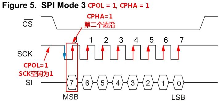
4 Operating Modes
Since data transmission is involved, both parties must clarify when the slave will sample the data sent by the master and when the master will read the data sent by the slave. For hardware SPI peripherals built into MCUs like STM32, this may not be critical, as it only requires configuration of the mode. However, for those using GPIO to simulate or implementing SPI timing with an FPGA, this is very important, involving the working modes of the SPI standard protocol. By varying the combinations of CPOL (Clock Polarity) and CPHA (Clock Phase), we can categorize them into four modes.
Generally, the working mode of the slave device is fixed, and the master must adopt the same working mode for both to communicate properly.
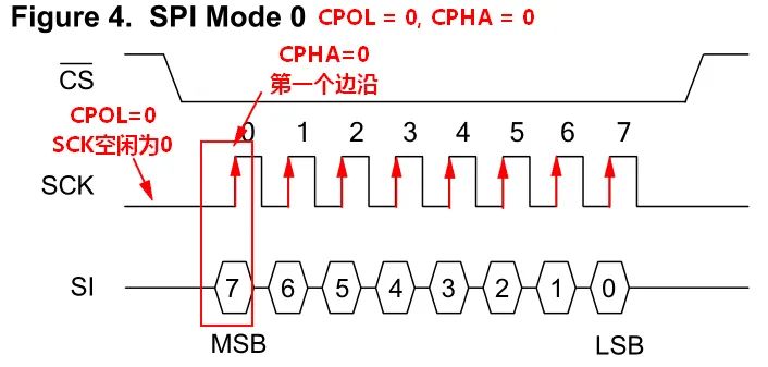
CPOL=0 indicates that SCK is 0 when idle.
CPOL=1 indicates that SCK is 1 when idle.
CPHA=0 indicates that data is valid on the first edge of SCK.
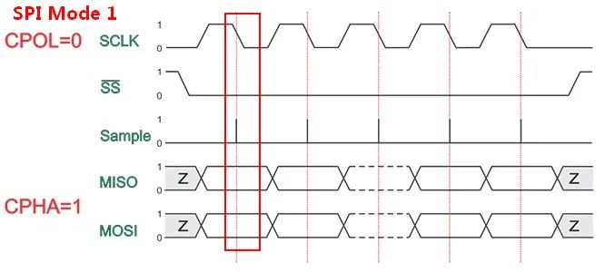
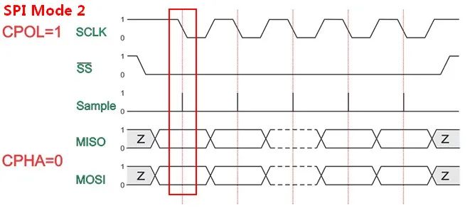
CPHA=1 indicates that data is valid on the second edge of SCK.Among these four modes, modes 0 and 3 are the most widely used, and most SPI devices support both modes. In fact, these details are not critical; the specific mode to use can be found in the device manual.
For example, in my recent work with a Cypress ferroelectric memory FM25V05, the official DataSheet indicates support for both SPI Mode 0 and Mode 3.

According to the subsequent timing diagram, we can see the read and write timing for SPI mode 0, where SCK is low when idle, and the master data is sampled by the slave on each rising edge, and data output follows the same principle.
For SPI mode 0, SCK is high when idle, and the master data is sampled by the slave on each rising edge, and data output follows the same principle.
Modes 1 and 2 follow the same logic. Mode 1 is CPOL=0, CPHA=1, SCK idle is 0, and data is valid on the second edge of SCK, which means it is valid on the falling edge of SCK.
Mode 2 is CPOL=1, CPHA=0, SCK idle is 1, and data is valid on the first edge of SCK, which means it is valid on the falling edge of SCK.
For some MCUs with built-in SPI hardware peripherals, setting the master SPI mode is very simple, requiring only the configuration of a few register values. It does not matter whether SCK is high or low, or whether it is the first or second edge, as long as you don’t need to remember if it equals 0 or 1. For example, the hardware SPI configuration for STM32F103:
SPI_InitTypeDef  SPI_InitStruct;

SPI_InitStruct.SPI_Mode =SPI_Mode_Master;       //Master
.....
SPI_InitStruct.SPI_CPOL =SPI_CPOL_High; //SCK idle high
SPI_InitStruct.SPI_CPHA =SPI_CPHA_1Edge;//SCK first edge valid
.....
SPI_Init(SPI2,&SPI_InitStruct);
However, implementing SPI timing in an FPGA requires strict timing control for SCK and data input/output.
Multiple Transmission Rates
The rate of SCK is the SPI transmission rate. The SPI protocol does not have a fixed rate, unlike IIC standard mode 100K, fast mode 400K, and high-speed mode 3.4M. The SPI transmission rate depends on the maximum rate supported by the device itself, which is described in the device manual. For example, for FM25V05:
 Maximum SCK clock frequency under different power supply voltages:
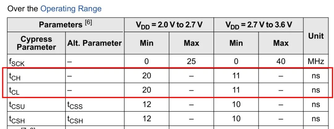
Basic Timing of SPI Protocol
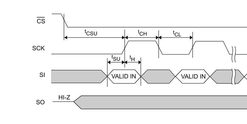
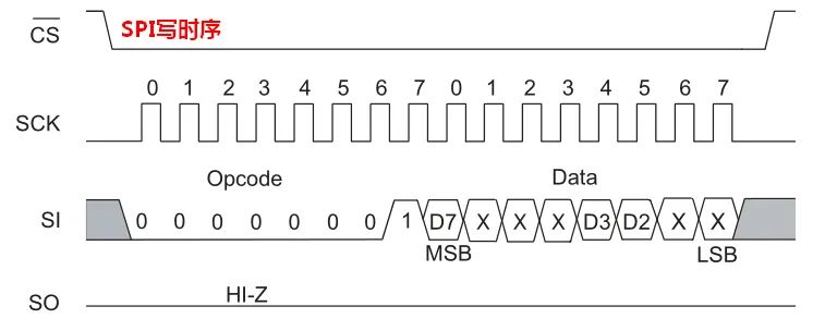
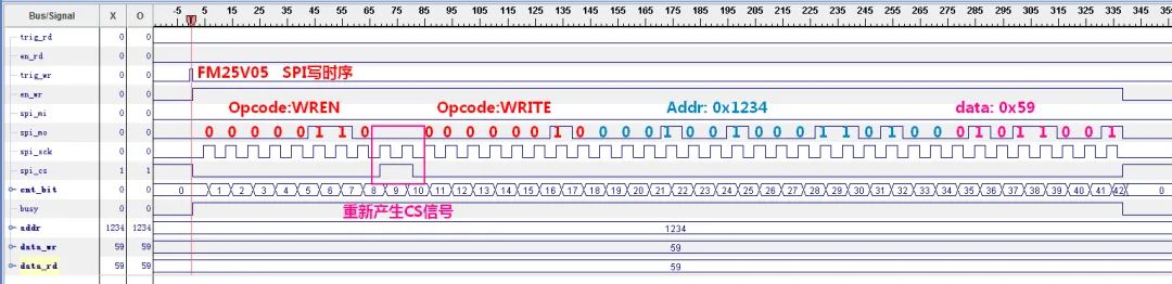
When CS is low, it indicates that the corresponding slave device is enabled. In each SCLK cycle, 1 bit of data can be transmitted, and the sampling moment depends on the SPI mode supported by the device. According to the control methods of different SPI devices, before performing formal data read and write operations, it is generally necessary to write a control word first, followed by the register address and data. Below is the write timing for the FM25V05 ferroelectric memory using SPI mode 0:
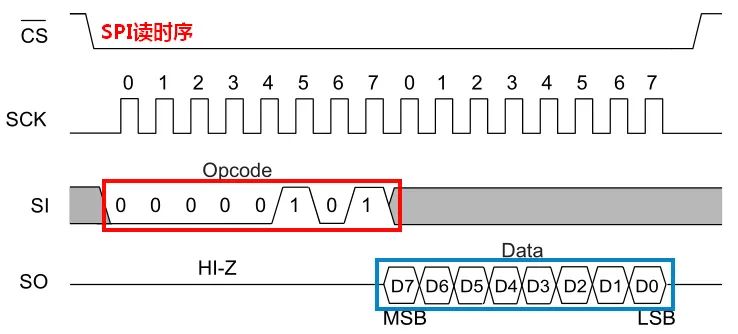
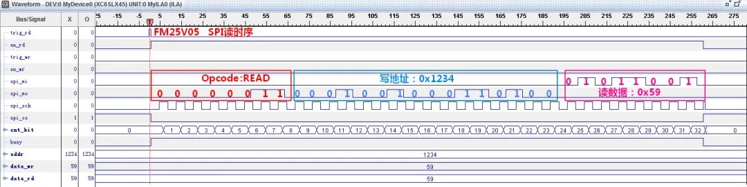
Read timing:
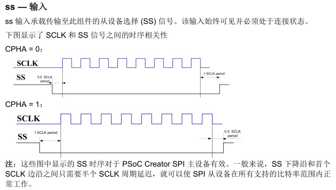
When using FPGA to implement SPI timing, there must be a certain delay between CS falling edge and SCLK first edge or CS rising edge and SCLK last edge, generally 0.5 SCLK cycles.
Some SPI slave devices support daisy chain connection mode, which saves GPIO and does not occupy too much wiring space, but not all SPI devices support daisy chain mode.
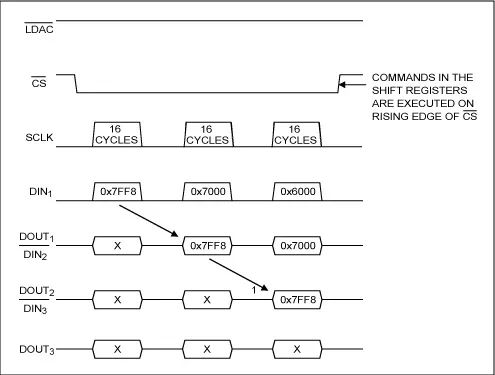
Control Timing:
Upgraded SPI Protocol
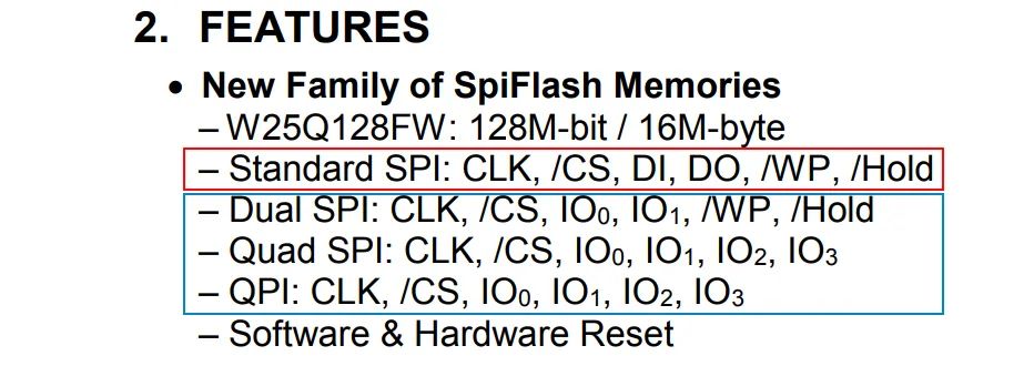
In the traditional standard SPI protocol, only 1 bit of data can be transmitted in one SCLK cycle. Can multiple bits be transmitted in one SCLK? The answer is yes. Motorola has developed various upgraded versions of the SPI protocol based on the existing standard 4-wire SPI protocol, enhancing data transmission efficiency by increasing the number of data lines. Currently, many Flash manufacturers support various SPI protocols.
Taking a commonly used SPI Flash ROM W25Q128FW as an example, its device manual states that in addition to the standard 4-wire SPI mode, it also supports Dual SPI, Quad SPI, QPI, where IO0/1/2/3 serve as bidirectional ports, significantly increasing data read and write rates.
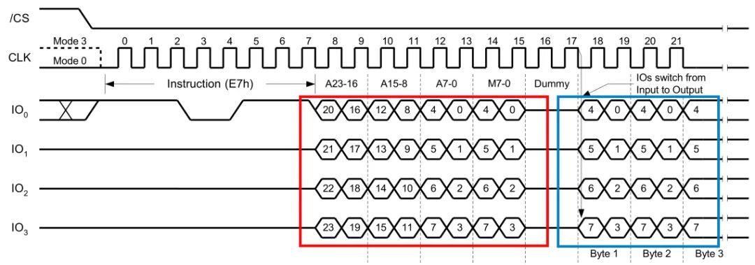
QSPI protocol read and write timing:
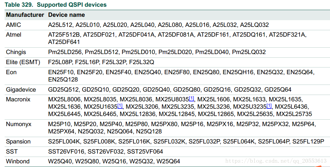
Some Flash chip models that support QSPI protocol:
FPGA Measured SPI Waveform
Implementing UART, SPI, IIC, and other serial timings in FPGA is commonly done using the state machine method, where each step is broken down into states, and the output or input reading is controlled based on the current state. Details must consider data alignment, setup and hold times, and transitions during exceptional conditions to avoid entering a dead loop or getting stuck in a state.
The waveform below is driven by an FPGA for a ferroelectric memory FM25V05 using the standard 4-wire SPI protocol, similar to the IIC interface operation: first write a control word, then write the address, and finally write or read data. The SCK clock frequency is 40MHz, and the actual read and write waveform captured by ChipScope shows that data changes in the middle of SCK low, and data must remain stable around the rising edge of SCK.
For SPI write timing, it is important to first write the enable command and then regenerate the CS signal. This part was quite tricky, and I only discovered the issue in the official example C code, indicating a misunderstanding of the timing in the manual.
For SPI read timing, first write the control word, then write the 16-bit address, and finally read the 8-bit data.
Comparison of SPI and IIC
-
SPI is full-duplex, while IIC is half-duplex.
-
IIC supports multi-master and multi-slave modes, while SPI can only have one master.
-
From a GPIO usage perspective, IIC occupies fewer GPIOs, saving resources.
-
SPI offers more flexible data bit widths, allowing for selection based on needs.
-
SPI protocol lacks a response mechanism, meaning the master cannot know if the slave has received the sent data, potentially leading to data loss if no measures are taken.
-
Because of the absence of a complex response mechanism, SPI can achieve very high rates (hundreds of megabits), with data transmission possible on every SCK, and methods like CRC checks can ensure both high-speed data transmission and accuracy.
-
IIC selects slaves via device addresses, and increasing the number of slaves does not increase GPIO usage, while SPI selects slaves via CS, requiring an additional GPIO for each slave. However, a decoder can be added for multi-slave control.
-
SPI protocol samples data on SCLK edges, while IIC samples on SCL high levels.
-
Both are mainly used for short-distance communication between board devices.
Conclusion
Implementing SPI timing using FPGA offers the greatest flexibility, allowing precise customization of timing based on needs, achieving very high rates, especially advantageous when driving multiple chips simultaneously. In scenarios requiring high-speed AD acquisition, using FPGA is essential. The challenge lies in the complexity of implementation, requiring meticulous debugging and simulation. While some ready-made IPs are available for FPGA, they still lack flexibility compared to STM32 and other MCUs, which can achieve master-slave modes, SPI modes, data bit widths, multiple rates, single-line and dual-line, half-duplex and full-duplex, DMA, etc., with just a few lines of configuration code. In summary, both FPGA and MCU have their advantages and disadvantages, and the choice should depend on requirements! Regardless of the controller used, as long as the timing is strictly controlled according to the data manual, there is no protocol that cannot be managed!
Author: wcc149
Source: Electronic Circuit Development Learning