We all know that typical IC components usually have two power pins, one is Vcc or Vdd, and the other is Gnd or Vss. However, modern MCUs often have multiple power pins. What is the reason for this?Taking a 100-pin MCU as an example, as shown in the figure below, we can see that it has 5 sets of VDD/VSS, and each set of VDD/VSS must be connected. In fact, these multiple VDD pins are internally connected together. Since this is the case, why don’t chip manufacturers just leave one set? Or, if multiple sets are provided, can we connect only one set externally? If this is possible, it would save pins and reduce external wiring.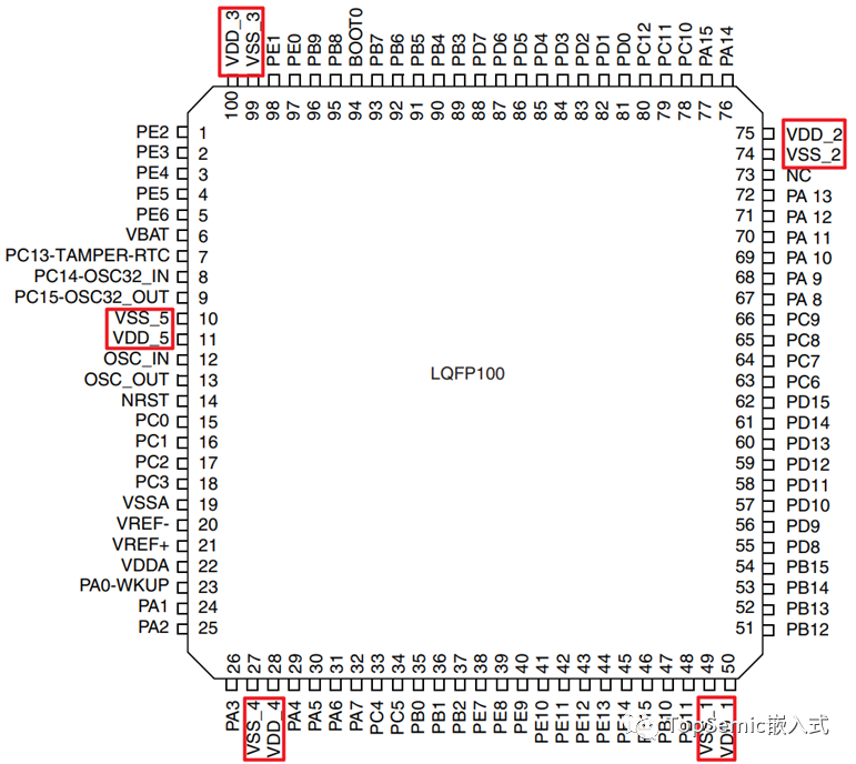 If only one set of VDD is connected externally, the current path inside the chip will be relatively long, as shown by the red lines in the figure below.
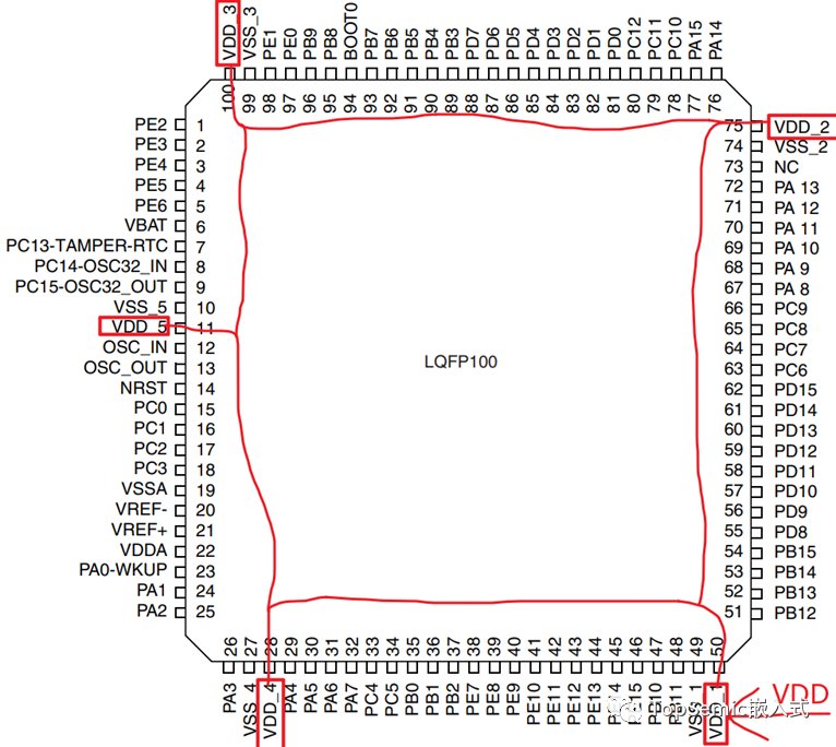 For high-frequency circuits, the VDD current will experience high-frequency transients (because the higher the frequency, the greater the current required), and at this time, the inductive reactance generated along the path will hinder the change in current. The longer the path, the greater the inductive reactance, which will more significantly impede the current, leading to voltage variations in the chip network, thus affecting the normal operation of the MCU system.For low-frequency or DC circuits, the long path has little impact. Therefore, early low-frequency MCUs only had one VDD, while multiple VDDs can reduce the inductive effect (the total inductance decreases when inductors are connected in parallel, and the shorter the path, the smaller the inductance).We can imagine the power supply process of the above chip as the process of irrigating a field; having only one water inlet is certainly not as effective as having multiple inlets supplying water simultaneously.In addition, here are a few more points:1) The analog peripherals of the MCU, such as ADCs, usually have a separate power supply, VDDA, because ADCs require as clean a power supply as possible to ensure the accuracy of conversion results. A separate line can avoid interference from noise from other power supplies.2) Multiple voltage requirements. Sometimes, different parts of the chip operate at different voltages. A typical example is a low-voltage core and high-voltage I/O. The core uses a lower voltage to reduce power consumption, while the I/O operates at a higher voltage to better connect with external circuits. In this case, multiple power supplies are also needed, which is common in complex SOC chips.3) Compared to a single VDD, having multiple VDDs reduces the current passing through each VDD pin, so the pins do not have to bear excessive current, enhancing reliability.
END
Source: TopSemic Embedded
Copyright belongs to the original author. If there is any infringement, please contact for removal.▍Recommended ReadingThe Japanese Operating System That Almost Dominated the World…Understanding the Differences Between hex, bin, and axf Files in One ArticleNo Foreign Authorization Needed! A Milestone in the Design of Domestic CPUs Has Arrived~→ Follow for More Updates ←