Today I checked the news and saw that ST has been breached? Then I noticed the new product from GD32. I took a quick look and felt that the Cortex®-M23 was somewhat unfamiliar, so I gathered some information to write about it before going to sleep.

On June 5, 2025, GigaDevice (stock code 603986), a leading semiconductor device supplier, announced the official launch of the value-oriented GD32C231 series, further expanding the product lineup of the Arm® Cortex®-M23 core. The GD32C231 series is positioned as “high-performance entry-level” and will provide more competitive solutions for applications such as small appliances, BMS battery management systems, small display devices, handheld consumer products, industrial auxiliary control, and automotive aftermarket.
GD32C231 Series MCU: The Ultimate Cost-Performance Choice
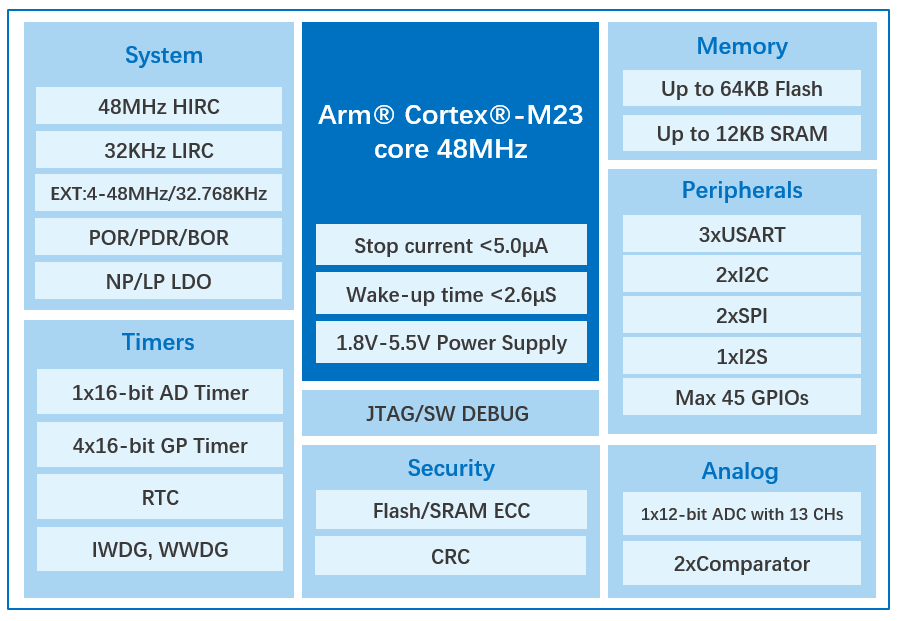
While maintaining excellent price competitiveness, it significantly enhances computing performance and peripheral specifications, achieving an ultra-high cost-performance upgrade. This series adopts Arm®’s advanced Cortex®-M23 core architecture, with performance improved by 10% compared to Cortex® M0+, a maximum frequency of 48MHz, and efficient processing capabilities such as single-cycle multiplication and integer division, greatly enhancing software execution efficiency.

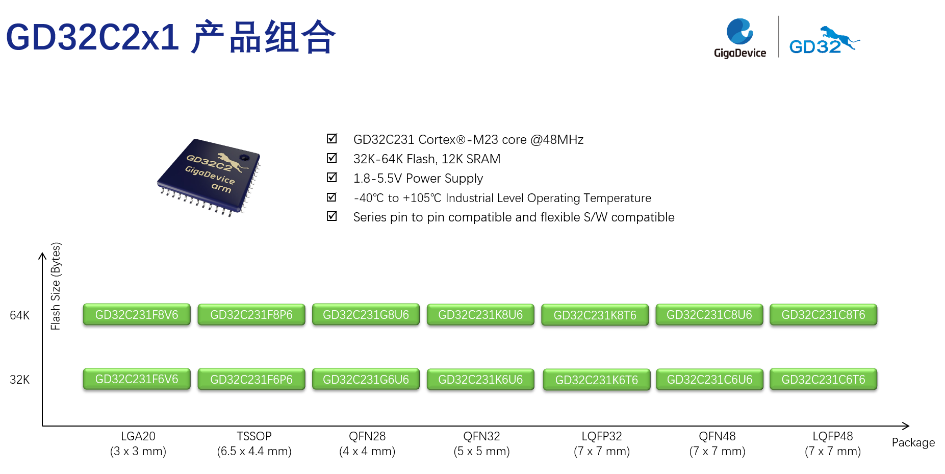
In terms of storage configuration, it is equipped with 32KB to 64KB of high-reliability embedded Flash and 12KB of low-power SRAM, with ECC error correction functionality across all storage areas. To meet the needs of different application scenarios, it offers various packaging options including TSSOP20/LGA20, QFN28, LQFP32/QFN32, and LQFP48/QFN48. Through highly integrated chip design, it effectively reduces the number of external components, providing users with a more cost-effective Bill of Materials (BOM) solution.
Perfect Balance of Wide Voltage, Low Power, and High-Speed Wake-Up
It features excellent power flexibility and low power characteristics, supporting a wide voltage supply of 1.8V to 5.5V and a wide temperature operating range of -40℃ to 105℃, making it suitable for various harsh environments. The chip provides multiple power management modes, with a current of less than 5μA in deep sleep mode while maintaining a fast response speed, with a wake-up time of 2.6μs, perfectly balancing low power consumption and real-time requirements, empowering battery-powered and portable device applications.
The GD32C231 also excels in safety and reliability: outstanding anti-static capability, reaching high standards of ESD protection with contact discharge of 8KV (CD) and air discharge of 15KV (AD); all Flash/SRAM adopts ECC error correction design to effectively prevent data errors; and it integrates a hardware CRC cyclic redundancy check module to ensure the integrity and reliability of data transmission. These features enable the chip to operate stably in industrial control, automotive electronics, and other fields with stringent safety requirements.
Highly Integrated Peripheral Resources Empowering Diverse Application Scenarios
It integrates rich peripheral resources, significantly enhancing system integration and application flexibility: it has a built-in 12-bit ADC (supporting 13 external channels) and 2 internal comparators to meet precision measurement needs; and provides up to 4 general-purpose 16-bit timers and 1 16-bit advanced timer. It is equipped with 2 high-speed SPI interfaces (supporting four-wire QSPI mode, with a rate of up to 24Mbps), 2 I2C interfaces (supporting Fast Mode+, with a rate of 1Mbit/s), and 3 UARTs (with a rate of 6Mbps), integrating 3 DMA controllers and 1 I2S to ensure efficient communication capabilities.
It also offers excellent GPIO expandability, supporting up to 45 GPIOs in a 48-pin package, significantly enhancing hardware design flexibility. These professional configurations enable the chip to easily handle diverse application scenarios in industrial control, consumer electronics, and more.
Alright, that’s what I saw on the official website. In summary, it’s a great MCU, but the UART of GD32 is very sensitive to timing.
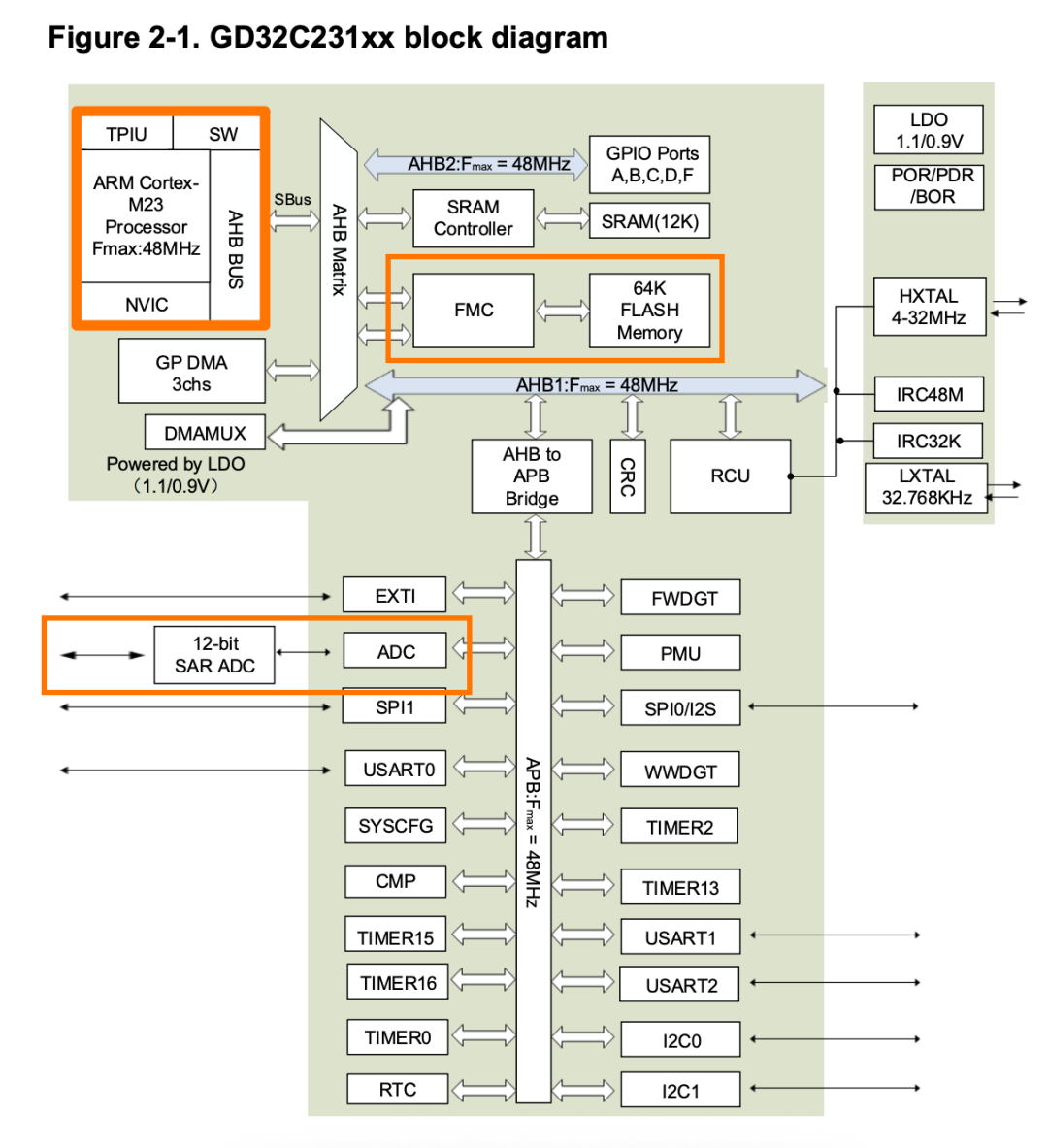
Next, let’s look at the core:
Let me state the conclusion first!
The Cortex-M23 is an entry-level processor designed specifically for ultra-low power, area-sensitive MCU applications (such as IoT nodes and secure sensors): particularly suitable for scenarios with certain security requirements but limited resources; compared to Cortex-M0+, it supports higher-level security isolation mechanisms such as TrustZone and MPU; compared to Cortex-M33, it is lighter in functionality and more suitable for applications with extreme area/power constraints.
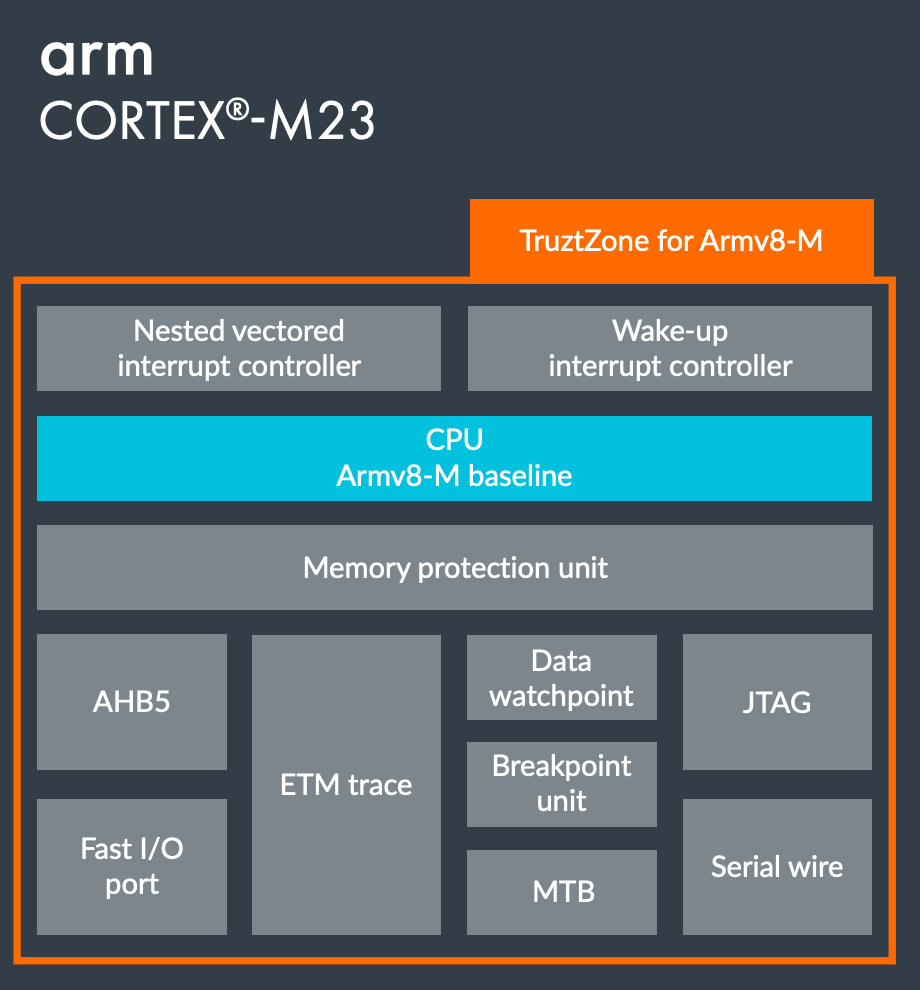
Overview
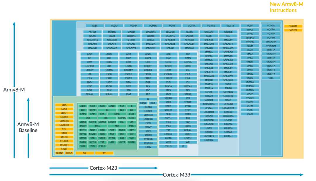
Processor Architecture: Based on Armv8-M Baseline, supporting Thumb/Thumb-2 instruction sets.
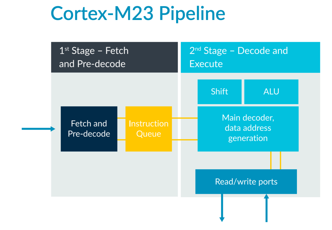
Pipeline Structure: Two-stage pipeline.
Bus Interface: AMBA AHB5 (using von Neumann architecture), optionally supports single-cycle I/O interface.
Security Mechanisms (TrustZone & Memory Protection)
I have always been skeptical about this until I wanted to steal firmware from an MCU, and then I realized that security is useful, haha.
Supports TrustZone for Armv8-M: divides the system into secure (Secure) and non-secure (Non-Secure) areas, with hardware-enforced resource isolation.
Supports Security Attribution Unit (SAU): up to 8 secure attribute regions.
Supports MPU (Memory Protection Unit): supports up to 16 memory protection regions in each security state; used to restrict illegal access and provide runtime memory protection.
TrustZone is the most important new feature of this architecture, explained in layman’s terms:
“I drew a ‘security line’ in the MCU; this side is the secure area (for running encryption programs, key management), and that side is the non-secure area (for running UI, Bluetooth stack).”
You cannot access each other’s content, just like a person cannot arbitrarily enter a bank vault.
To access secure content, you must go through the “secure gateway function” (Secure Gateway, <span>SG</span> instruction); there is a “Security Attribution Unit SAU” that specifically defines whether each memory segment is secure/non-secure; each has its own stack (to prevent stack collision); interrupts can be configured to be received only by “secure code”.
Interrupt Control (NVIC)
Supports 1 to 240 external interrupt sources, with 4 levels of priority.
Non-Maskable Interrupt (NMI) is supported.
Supports WIC (Wake-up Interrupt Controller): low-power wake-up function.
Integrates Wait For Interrupt (WFI) and Wait For Event (WFE), supporting Sleep-On-Exit mode.
Debug & Trace
Supports JTAG and Serial Wire Debug (SWD).
Optional support:
ETM (Embedded Trace Macrocell): instruction-level tracing;MTB (Micro Trace Buffer): simplified tracing;CTI (Cross Trigger Interface): debugging interaction component; configurable for up to 4 breakpoints and 4 watchpoints (wow, 4? M0 seems to only have 2).
Performance Features
Multiplier: 32×32 bit multiplication, supports single-cycle implementation;
Divider: supports fast division (17 cycles) or slow division (34 cycles);
Instruction Dispatch: limited dual-issue support;
Fast interrupt context switching, supports nested interrupts and precise exception handling (precise bus error).
Peripheral Interfaces & System Integration
Supports AHB5 interface + optional single-cycle I/O interface (high-performance GPIO).
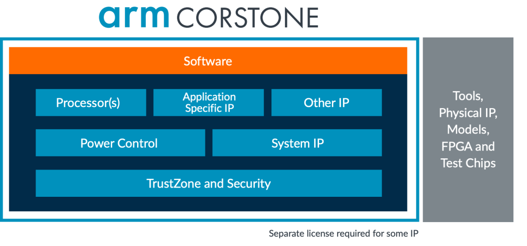
Optional use of Arm Corstone platform:
Provides a set of SoC reference subsystem designs, including the main control, security module, and peripheral components;
Can be adapted to PSA certified platforms.
Implementation Options
This is likely aimed at upstream, and we don’t know if we can use it:
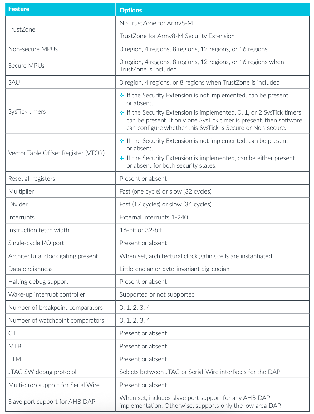
| Configuration Options | Optional Values/Description |
|---|---|
| TrustZone Support | Yes/No |
| Number of MPU Regions | 0, 4, 8, 12, 16 (divided into Secure/Non-secure) |
| Number of SAU Regions | 0, 4, 8 |
| SysTick Timer | 0, 1, 2 (with or without security extension) |
| Number of Interrupts | 1 to 240 |
| VTOR Register | Optional |
| Instruction Width | 16-bit / 32-bit |
| Multiplier | Fast/Slow |
| Divider | Fast/Slow |
| Trace (ETM/MTB/CTI) | Optional Enable |
| Interrupt Wake-Up Controller WIC | Optional Enable |
| Debug Method | JTAG / Serial Wire |
Power & Area
For comparison under different processes:
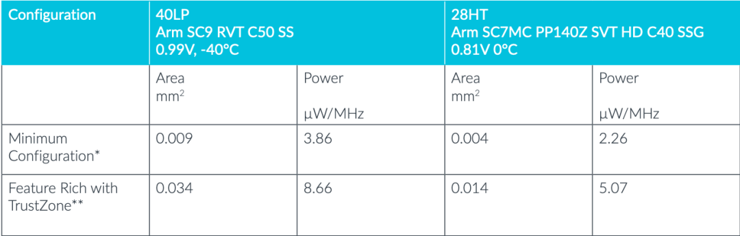
| Configuration | Area (mm²) | Power (µW/MHz) |
|---|---|---|
| Minimum Configuration (No Security Features) | 0.009 | 3.86 |
| Rich Configuration (Including TrustZone) | 0.034 | 8.66 |
| 28nm Process Minimum Configuration | 0.004 | 2.26 |

Let me briefly talk about this V8 programming model (just a little bit):
Armv8-M is an architecture designed specifically for microcontrollers, divided into two configurations:
Armv8-M Baseline (like Cortex-M23): lighter;
Armv8-M Mainline (like Cortex-M33): supports more debugging and DSP features.
Backward compatible with Thumb/Thumb-2 instruction sets, for efficient code density.
Core features include: streamlined pipeline; supports exception nesting, tail chaining; flexible interrupt priority; hardware stack management; security extension: TrustZone for Armv8-M (hardware-level isolation mechanism).
I feel like I can’t learn anymore, goodbye.