1. What is a Dielectric?
A dielectric refers to a substance or space that can transmit force, energy, or information under specific conditions. In physics and engineering, dielectrics typically refer to solids, liquids, or gases that can transmit mechanical waves, electromagnetic waves, etc. For example, in acoustics, air, water, and solids can serve as media for sound wave propagation; in electricity, conductors and insulators can act as media for current transmission; in optics, substances like air and glass can serve as media for light propagation. The properties of the dielectric affect the wave propagation speed, attenuation, and other factors.
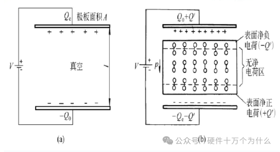
Under the influence of an electric field, all substances that can be polarized are referred to as dielectrics. Dielectrics are used in the electronics industry to make substrates for integrated circuits, capacitors, etc. If a dielectric is placed in a parallel electric field, it can be observed that charges are induced on the surface of the dielectric, with negative charges induced near the positive plate and positive charges induced near the negative plate. This phenomenon of induced charge generation in dielectrics under the influence of an electric field is called dielectric polarization. The reason for the induced charge is the separation of the centers of positive and negative charges of the particles (atoms, molecules, ions) within the dielectric under the electric field, forming dipoles. Different dipoles have different electric dipole moments, and the direction of the electric dipole moment aligns with the direction of the external electric field.
2. What is the Dielectric Constant?
The dielectric constant is the ratio of the capacitance of a capacitor made with an insulating material as the dielectric to that made with a vacuum as the dielectric, both having the same dimensions.
It represents the amount of electrostatic energy stored per unit volume in a unit electric field. It characterizes the ability of a dielectric to polarize and store charge, and is a macroscopic physical quantity.
Dielectric loss refers to the energy loss exhibited by a dielectric placed in an alternating electric field, manifested as internal heating (temperature increase).
It is usually denoted by the Greek letter ε and describes a physical quantity that reflects the response of the dielectric in an electric field. It is the ratio of the ability of the dielectric to store electric field energy compared to that in a vacuum. The dielectric constant reflects the capacitance of the dielectric relative to that of a vacuum.
Specifically, the dielectric constant describes the ability of a dielectric to respond to an electric field. When a dielectric is placed in an external electric field, the larger the dielectric constant, the higher the degree of polarization of the dielectric molecules or atoms under the electric field force, thus storing more electrical energy in the dielectric. The dielectric constant is usually a positive value, indicating that the polarization effect of the dielectric will enhance the effect of the electric field; however, there are cases where it can be negative, such as in metals, where the dielectric constant can change from positive to negative as frequency increases, a phenomenon known as surface plasmon resonance in metals.
The dielectric constant can also be expressed in terms of the relative dielectric constant, which is the ratio of the dielectric constant to that of a vacuum:
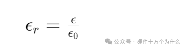
Where εr is the relative dielectric constant, and ε0 is the dielectric constant of vacuum, approximately equal to 8.854 × 10⁻¹² F/m.
The dielectric constant of a PCB (Printed Circuit Board) depends on the substrate material used. The substrate materials for PCBs are typically high-dielectric constant insulating materials, commonly including:
-
FR-4: This is one of the most common PCB substrate materials. It is a glass fiber reinforced epoxy resin composite with a dielectric constant of approximately 4.0 to 4.5.
-
FR-1, FR-2, FR-3: These are also commonly used PCB substrate materials, with dielectric constants typically slightly higher than FR-4, around 4.0 to 5.0.
-
PTFE (Polytetrafluoroethylene): PTFE is a low-dielectric constant material, usually used for high-frequency applications, with a dielectric constant of about 2.1 to 2.3.
-
RO4000 Series: This is a series of PCB substrate materials specifically designed for high-frequency applications, with dielectric constants typically ranging from 3.38 to 3.66.
These dielectric constants are measured at specific frequencies and may vary due to factors such as material manufacturers, board thickness, and layer stacking methods. The choice of appropriate PCB substrate material depends on the specific application requirements, including operating frequency, signal speed, signal integrity, and other considerations.
3. What is Dielectric Loss?
Dielectric loss refers to the energy loss caused by the dielectric material under the influence of an electric field due to the dielectric conductivity and the hysteresis effect of dielectric polarization. It is also called dielectric loss, abbreviated as dielectric loss.
When a dielectric is subjected to an external electric field, internal heating occurs, indicating that some electrical energy has been converted into thermal energy and dissipated. The energy consumed by the dielectric due to heating in a unit time is called the dielectric loss power, or simply dielectric loss. Dielectric loss is one of the important quality indicators for dielectrics used in alternating electric fields. Dielectric loss not only consumes electrical energy but also causes components to heat up, affecting their normal operation. If the dielectric loss is too high, it can even lead to overheating and insulation failure of the dielectric, so from this perspective, the smaller the dielectric loss, the better.
4. How is Dielectric Loss Generated?
Dielectric loss is a phenomenon of energy loss in insulating materials caused by the action of an electric field. It is mainly caused by the dielectric’s conductivity and the hysteresis effect of polarization. When an insulating material is placed in an electric field, the electric field causes the charge distribution within the material to rearrange, resulting in polarization. However, this polarization is not instantaneous and has a certain lag time. When the electric field changes, the polarization of the dielectric also lags, leading to energy loss within the dielectric.
The main mechanisms of dielectric loss are conductive loss and polarization loss.
-
Conductive Loss: Free charges in the dielectric move under the influence of the electric field, generating current and causing energy loss.
-
Polarization Loss: The polarization in the dielectric is affected by the electric field, but the polarization does not immediately follow the changes in the electric field, leading to energy loss within the dielectric.
Various forms of loss work together. Since the causes of dielectric loss are multifaceted, the forms of dielectric loss are also diverse. In addition to conductive loss and polarization loss, there are other causes of dielectric loss.
1) Leakage Conductive Loss
Leakage conductive loss, also known as conductive loss, occurs because real insulating materials are not perfect ideal dielectrics. Under the influence of an external electric field, some charged particles will move, causing a weak current. This small current is called leakage current, and when it flows through the dielectric, it causes heating and energy loss. This type of dielectric loss caused by conductivity is referred to as “leakage conductive loss.” Since real dielectrics always have some defects, there will always be some charged particles or vacancies, leading to leakage conductive loss under both direct current and alternating current fields.
2) Polarization Loss
During slow polarization of the dielectric (such as relaxation polarization, space charge polarization, etc.), energy loss occurs as charged particles overcome thermal motion under the influence of the electric field.
Some dielectrics also produce losses during electric field polarization, generally referred to as polarization loss. Displacement polarization stabilizes quickly (about 10-16 to 10-12 s), which is considered very short in the radio frequency range (below 5 × 10¹² Hz) and does not consume energy. Other slower polarizations (such as relaxation polarization, space charge polarization, etc.) take longer (10-10 s or longer) to reach a stable state under the influence of the external electric field, thus causing energy loss.
If the external frequency is low, all polarizations in the dielectric can completely follow the changes in the external electric field, resulting in no polarization loss. If the external frequency is high, the polarization in the dielectric cannot keep up with the changes in the external electric field, leading to polarization loss.
Polarization: In a dielectric, when an external electric field acts on the dielectric, the molecules or atoms within the dielectric are influenced by the electric field and rearranged, resulting in an electric dipole moment within the dielectric. This process is called polarization. Polarization generates a spontaneous electric field within the dielectric that opposes the direction of the external electric field.
Polarization Current: When the external electric field changes, the polarization within the dielectric also changes, generating a current proportional to the rate of change of the electric field. This current is called the polarization current, and its direction generally aligns with the direction of polarization.
Weakly Bound Charge-Induced Polarization Current: This phrase refers to the fact that when the dielectric is under the influence of an external electric field, the polarization current within the dielectric is mainly caused by weakly bound charges within the dielectric. Weakly bound charges refer to charges within the atoms or molecules of the dielectric that are weakly bound between electrons and atomic nuclei. These charges will displace under the influence of the external electric field, leading to polarization and thus generating polarization current.
3) Ionization Loss
Ionization loss (also known as free loss) is caused by gas. When the electric field strength exceeds the ionization threshold of the gas in the pores of solid dielectrics, energy is absorbed due to the ionization of the gas, resulting in loss, which is referred to as ionization loss.
4) Structural Loss
In high-frequency electric fields and low temperatures, a type of dielectric loss closely related to the density of the internal structure of the dielectric is called structural loss. This type of loss is not significantly affected by temperature, and the power loss increases with frequency.
Experiments show that tightly structured crystalline materials have low structural loss, but when certain factors (such as the introduction of impurities, rapid cooling of samples, etc.) cause the internal structure to become loose, the structural loss can significantly increase.
5) Dielectric Loss Due to Macroscopic Structural Inhomogeneity
Most engineering dielectric materials are inhomogeneous dielectrics. Due to the different dielectric properties of each phase, it is possible for a large amount of free charge to accumulate between two phases, causing an uneven electric field distribution and resulting in higher local electric field strength, leading to higher losses. However, from the perspective of the overall dielectric, the dielectric loss must lie between the maximum loss of one phase and the minimum loss of another phase.
5. Parallel Capacitor Model
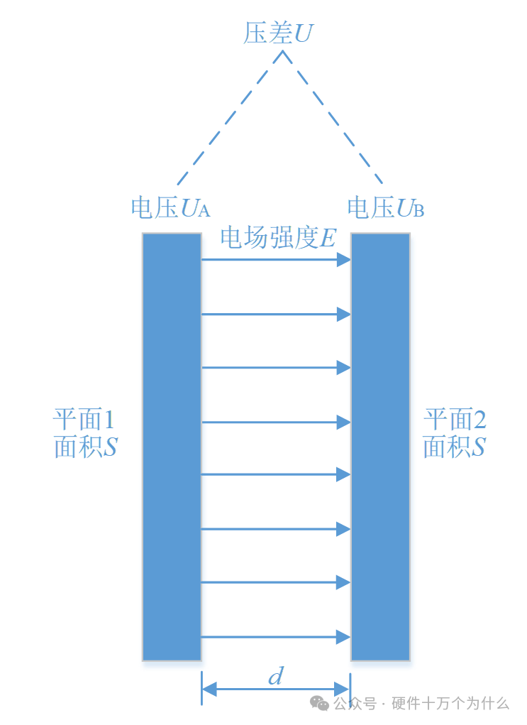
The simplest structure of a capacitor can be formed by two closely spaced conductors with a layer of insulating dielectric in between. When a voltage is applied across the two plates of the capacitor, it will store charge, making the capacitor an electronic component for charging and discharging. The capacitance is a measure of how much charge the capacitor can store. The capacitance of a parallel plate capacitor can be calculated using the following formula.
Where C is the capacitance in Farads (F); Q is the charge stored on one electrode in Coulombs (C); U is the potential difference across the two electrodes in Volts (V); ε is the dielectric constant of the insulating medium; S is the area of the metal plates in square meters (m²); and d is the distance between the conductors in meters (m).
From the formula, it can be seen that the charge Q stored on one electrode is determined by both internal and external factors. The internal factor is C, the ability of the capacitor to hold charge; the external factor is the external voltage, the pressure applied to the charge. At the same voltage, the amount of charge a capacitor can hold is fixed, and the capacitance value indicates this ability, which is influenced by the area S of the conductors and the distance d between them, affecting the interaction force of the charges. It has also been found that placing different materials with different dielectric constants ε between the two conductors will also affect the capacitance value, thus changing the formula.
The capacitance of a parallel plate vacuum capacitor:
In some cases, such as in vacuum or air, when the dielectric constant between the two parallel plates is considered to be 1, the propagation of the electric field is considered to be uniformly distributed, the capacitance formula for the capacitor is usually written as:
The inclusion of 4π in the denominator of the capacitance formula depends on the specific context and assumptions of the problem.
In some cases, such as in vacuum or air, when the dielectric constant between the two parallel plates is considered to be 1, the propagation of the electric field is considered to be uniformly distributed, the capacitance formula for the capacitor is usually written as:
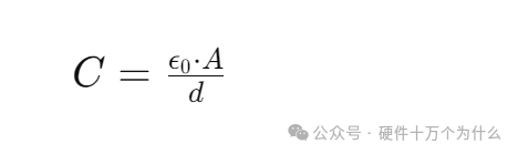
Where C is the capacitance (in Farads, F), ε0 is the dielectric constant of vacuum (in Farads per meter, F/m), A is the area of the plates of the parallel plate capacitor (in square meters, m²), and d is the distance between the plates (in meters, m).
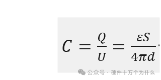
In other cases, when the dielectric is not vacuum or air but has different dielectric constants, the denominator in the formula may include 4π. This is because, in general, the electric field will change due to the presence of the dielectric, and the effect of the dielectric on the electric field needs to be considered.
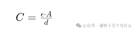
For parallel plate capacitors, considering the effect of the dielectric on the electric field will lead to changes in the strength of the electric field, which is usually described by the dielectric constant. When the dielectric is uniform, isotropic, and has no free charges, we can use the following formula to calculate the capacitance:
Where C is the capacitance, ε is the dielectric constant, A is the area of the plates of the parallel plate capacitor, and d is the distance between the plates. In this case, ε usually represents the relative dielectric constant, which is the dielectric constant of the medium relative to that of vacuum. However, in this formula, there is no factor of 4π.
When the dielectric is not uniform, isotropic, or when there are complex situations such as polarization and charge in the electric field, we need to consider the diffusion of the electric field and the change in the distribution of electric field strength. In this case, it is usually necessary to introduce 4π to describe the divergence of the electric field. In such cases, the capacitance formula may become more complex, requiring consideration of the dielectric’s effect on the electric field, and the formula may include the factor of 4π.
Therefore, simply put, if the dielectric is uniform, isotropic, and has no free charges, 4π is usually not needed. However, if the dielectric does not meet these conditions, or if there are special cases that require consideration of the diffusion effect of the electric field, 4π may need to be introduced.
6. What is the Dielectric Loss Angle?
First, let’s consider the ideal capacitor in a vacuum when we apply an alternating electric field to the capacitor.
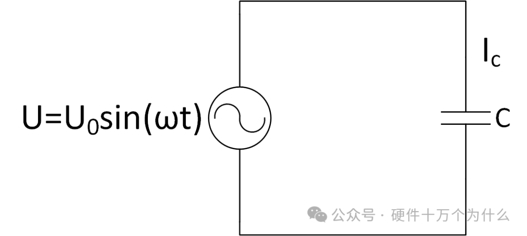
① Ideal Case
The capacitance of a parallel plate vacuum capacitor:
When an alternating voltage with angular frequency ω is applied to the capacitor, ω=2πf:
U=U0sin(ωt)
We can write it in complex form:
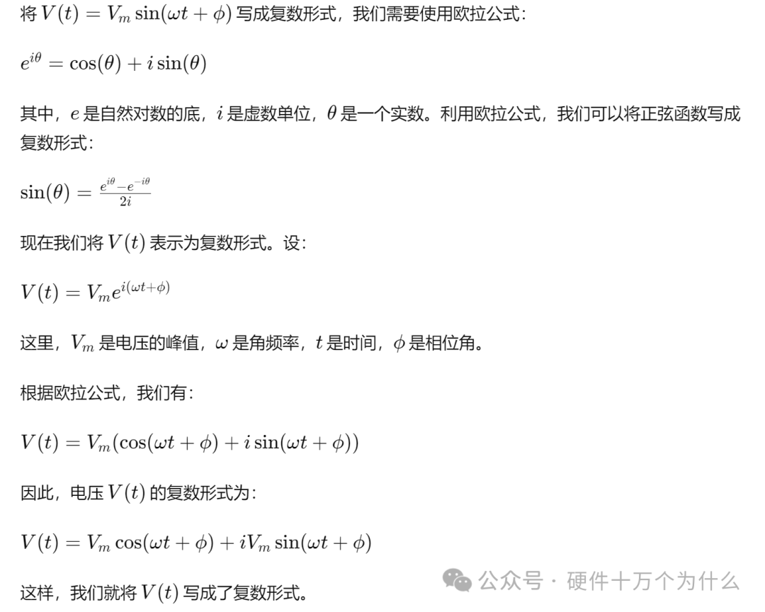
U=U0 eiωt
According to the current being the charge passing through per unit time, and Q=C0U
Then:
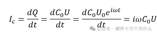
This Ic is the capacitive current, which is the current charging the capacitor. The phase of this current, from the complex perspective, is equivalent to U multiplied by a pure imaginary number, resulting in a phase shift of 90°. From the trigonometric function perspective, the sine function differentiates to cosine, also resulting in a phase shift of 90°. This current acting on an ideal capacitor does not produce thermal or chemical effects.
This current is merely a phase shift, hence also referred to as displacement current. It leads the voltage U by 90° in phase. This is a non-dissipative current.
If an ideal dielectric with a dielectric constant εr is embedded between the two plates of the capacitor, then
C=εr*C0
After embedding the dielectric, the current changes to I’C
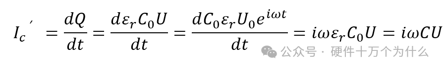
After adding the dielectric, the current phase still leads the voltage U by 90°.
At this point, we can still consider the ideal dielectric as not affecting energy consumption, i.e., the new charged dielectric does not consume energy.
② Non-Ideal Case, Actual Materials
In reality, after adding a dielectric, there will definitely be energy loss. This is what we mentioned in points three and four—dielectric loss. With a dielectric, there will be dielectric loss.
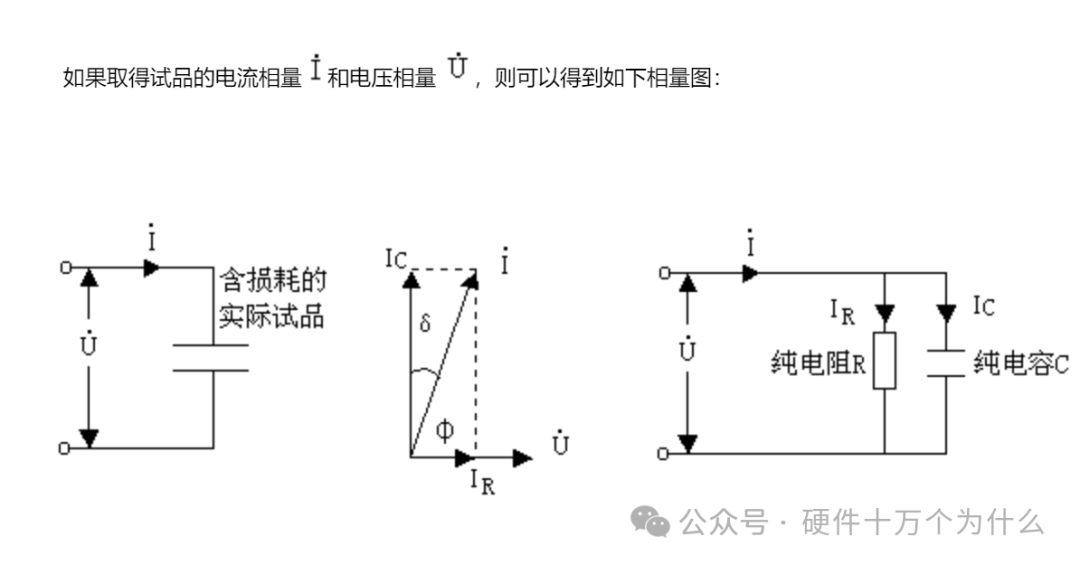
We embed an actual dielectric (non-ideal) material into the parallel plate capacitor and apply alternating voltage U; at this point, the phase of the current and voltage is no longer 90°.
We can simplify the model to understand it as “leakage current” in the dielectric, which exists as resistance, or can be understood as existing “conductance”.
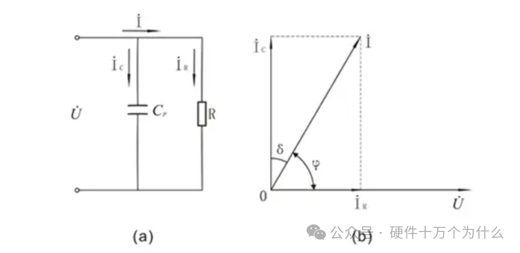
(a) Equivalent circuit of leakage current resistance in parallel;
(b) Phasor diagram of the parallel equivalent circuit
At this point, we have created a conductive current path, which we denote as G, the reciprocal of resistance R.
The current component through the conductance is equal to GU, which is the current through the conductance or through the leakage current resistance.
For actual dielectrics, in addition to the ideal capacitive charging current Ic, there is also a leakage current conductance component GU, which can be simply understood as being mainly composed of leakage current Idc and polarization current Iac caused by weakly bound charges.
GU≈Iac+Idc, other factors of dielectric loss are relatively small and can be ignored.
At this point, the total current during the charging of the dielectric capacitor is
I=Ic+GU=iωCU+GU
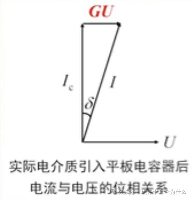
Due to the presence of Iac and Idc, the phase angle of the total current no longer remains 90°; this angle changes to 90°-δ, where the changed offset angle δ is caused by the loss, which is the angle we denote as the loss angle—dielectric loss angle.
The dielectric loss factor (tan δ) and the dielectric loss angle (δ) have a direct trigonometric relationship. The dielectric loss angle is an angle that describes the energy loss generated by the dielectric under the influence of an electric field, while the dielectric loss factor is the tangent of the dielectric loss angle. Their relationship can be expressed by the following formula:
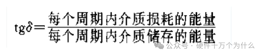
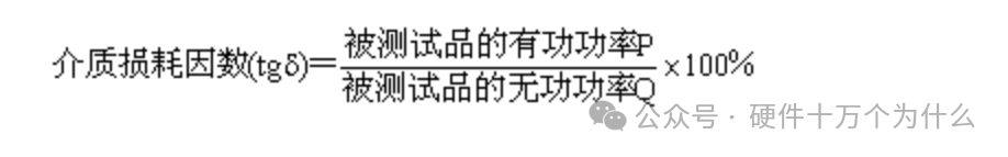
The dielectric loss angle (δ) can be calculated using the inverse trigonometric function of this formula: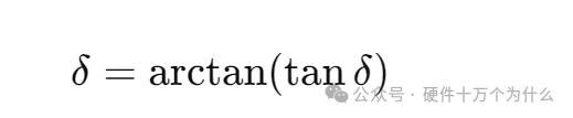
The dielectric loss angle is usually expressed in radians, representing the angular difference between the phase change of the electric field in the dielectric and the change in electric field strength. In circuit analysis and materials engineering, the dielectric loss angle and the dielectric loss factor are often used to describe the energy loss of dielectrics in alternating electric fields.
The tangent of the loss angle represents the magnitude of energy consumed to obtain a given stored charge, which is an important evaluation parameter for dielectrics used as insulating materials. To reduce dielectric loss, it is desirable for materials to have a smaller dielectric constant and a smaller loss tangent. The reciprocal of the loss factor Q=(tan δ)-1 is referred to as the quality factor of the dielectric under high-frequency insulation applications, and its value should be high.
7. Dielectric Loss Angle of PCB
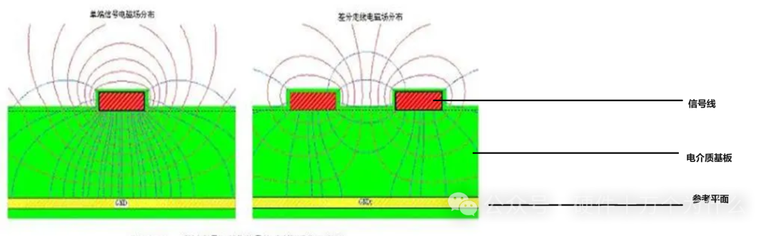
When an epoxy resin printed circuit board material (without copper cladding on both sides) is placed in a microwave oven and heated at full power for 1 minute, it will be significantly heated by microwaves. Similarly, a ceramic plate or heat-resistant glass placed in the microwave will also be heated. In fact, almost any insulating material can be heated in a microwave oven. The heat absorbed by insulating materials in an alternating electric field is proportional to the dielectric loss factor of that material. When insulating materials serve as the insulating medium for transmission lines, dielectric loss translates into signal attenuation. The higher the dielectric loss, the greater the resulting attenuation.
If our signal line is attached to a dielectric substrate, and the signal is a high-frequency alternating electromagnetic field, the effect is similar to placing the substrate in a microwave oven, just with less energy.
Dielectric loss is a function of frequency. When the frequency of digital devices is below 1 GHz, the dielectric loss of epoxy resin (FR-4), commonly used as PCB material, can be neglected. Under high-frequency conditions, the dielectric loss of FR-4 becomes significant. For high-frequency circuits, designers should choose ceramic substrate materials, such as alumina, which have better dielectric loss factors at gigahertz frequencies.
For FR-4 materials, designers of analog circuits are more concerned about its dielectric loss at low frequencies. When constructing a high Q-value circuit, where the amplitude of the oscillating signal does not decay over multiple cycles, this loss issue becomes very serious. Digital circuits generally avoid high Q-value circuit structures, so they are not very sensitive to this dielectric loss. For digital circuit board applications below 1 GHz, dielectric loss can be neglected.
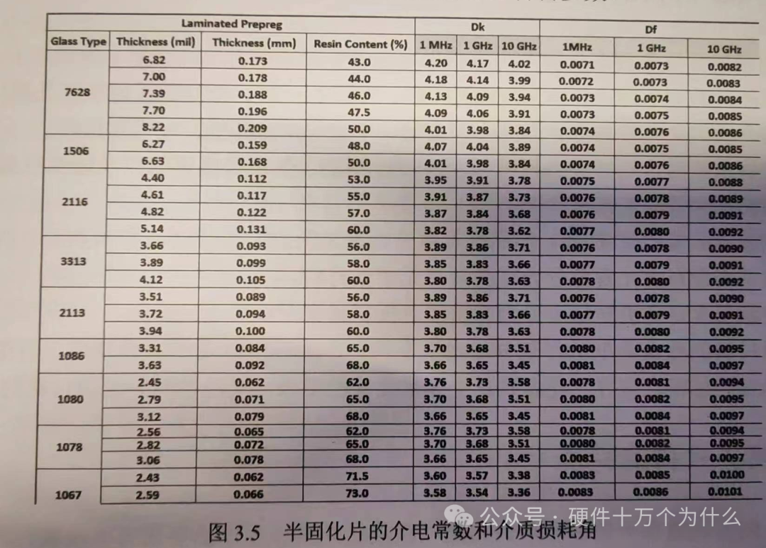
Both the dielectric constant and the dielectric loss angle vary with frequency, so when stating the dielectric constant and dielectric loss angle of a certain dielectric, the frequency must be specified. The specifications of materials will also clearly indicate this, as shown in the following figure for some material parameters of ITEO IT-170GRA prepreg.
A common method is to accurately measure the S-parameters of transmission lines on PCB boards using a network analyzer, and then fit the frequency-varying dielectric constant and dielectric loss angle using ADS. The following figure shows the frequency variation curves of the dielectric constant and dielectric loss of Shengyi Technology’s material S6.
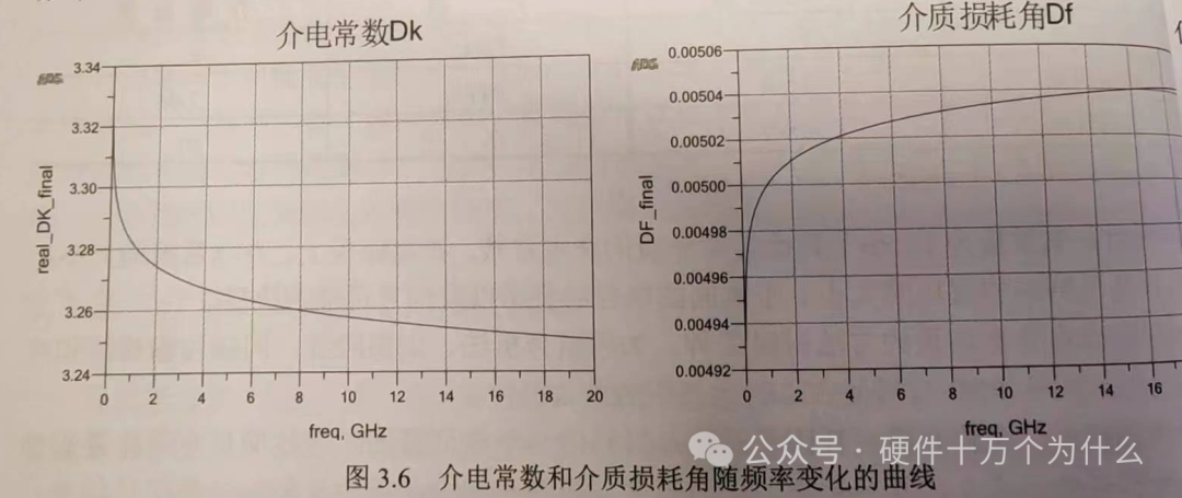
The above two figures are sourced from “ADS Signal Integrity Simulation and Practice (Second Edition)”
Based on ADS2023, “ADS Signal Integrity Simulation and Practice” Second Edition
Long press the QR code to learn more about the book details
My process of enhancing my understanding of PCB design【1】Driven by interest and passion
My process of enhancing my understanding of PCB design【2】Should hardware engineers draw PCBs themselves?
My process of enhancing my understanding of PCB design【3】How long should PCB traces be?
My process of enhancing my understanding of PCB design【4】How wide should PCB traces be?
My process of enhancing my understanding of PCB design【5】Inner layers of PCB
My process of enhancing my understanding of PCB design【6】Via holes
My process of enhancing my understanding of PCB design【7】Can PCB traces have sharp angles and right angles?
My process of enhancing my understanding of PCB design【8】Should dead copper be retained? (PCB islands)
My process of enhancing my understanding of PCB design【9】Can vias be placed on pads?
My process of enhancing my understanding of PCB design【10】PCB materials,What does FR4 refer to?
My process of enhancing my understanding of PCB design【11】Solder mask,Why is green oil mostly green?
My process of enhancing my understanding of PCB design【12】Steel mesh
My process of enhancing my understanding of PCB design【13】Pre-layout
My process of enhancing my understanding of PCB design【14】Principles of PCB layout and routing
My process of enhancing my understanding of PCB design【15】Cross-segment routing
My process of enhancing my understanding of PCB design【16】Signal reflection
My process of enhancing my understanding of PCB design【17】Dirty signals
My process of enhancing my understanding of PCB design【18】Surface treatment processes such as gold plating, tin spraying, etc.
My process of enhancing my understanding of PCB design【19】Line spacing
My process of enhancing my understanding of PCB design【20】Placement of capacitors
My process of enhancing my understanding of PCB design【21】Crosstalk
PCB flying probe testing
Overview and simulation of FPC
Why do PCBs deform and bend? How to solve it?
Understanding “Characteristic Impedance” in one article
PCB stacking design
High-speed circuit PCB return path
Power handling and plane segmentation in PCB design
Sawtooth PCB routing—Tabbed routing
Tomorrow, Hard Ten customer service will start work, and the Hard Ten website will resume shipping
www.hw100k.com
Click the original link to enter “Hard Ten Classroom”