Japan’s Rapidus has successfully taped out a 2 nanometer GAA test chip, with plans for mass production in 2027, utilizing ASML‘s EUV tools for manufacturing. This node has achieved all the required electrical characteristics set initially, with the IIM-1 fab expected to produce about 25,000 wafers per month. By 2027, Rapidus aims to fall behind TSMC and even Intel by one or two nodes. Therefore, the company hopes to stand out in the competition by becoming the most agile player in the field, claiming to reduce the waiting time for custom wafers from three months to just 50 days, with wafer production time only 15 days.
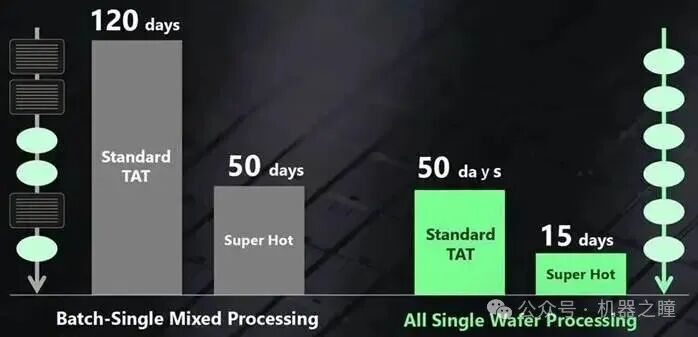
In the 1980s, Japanese chip manufacturers dominated the global market. However, with market developments and the emergence of new competitors in East Asia, Japan has gradually fallen behind in the advanced logic chip manufacturing sector. Today, Japan is lagging up to twenty years behind the world leaders. Even if Rapidus successfully produces a 2 nanometer chip prototype, this alone does not guarantee success in mass production. They will soon enter a phase commonly referred to as “the valley of death,” which is the critical gap between R&D and commercialization.
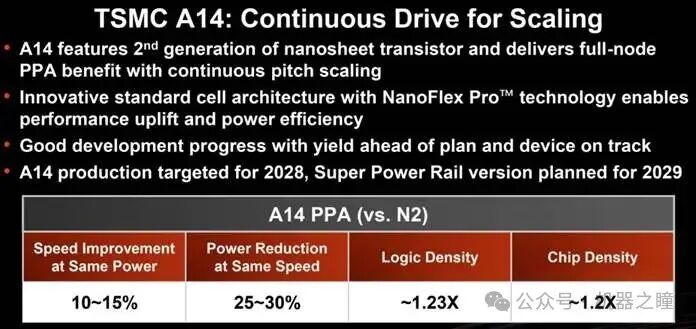
On the other hand, TSMC’s Central Science Park 1.4 nanometer advanced process plant is moving ahead. The Central Science Park Administration stated yesterday (the 27th) that the public works related to the second phase of the park’s expansion will be completed by the end of September. Supply chain sources indicate that TSMC’s new plant is expected to start construction in October, with an estimated total investment amounting to 233.8 billion to 350.8 billion RMB. Four factories are planned, with the first factory expected to complete risk production by the end of 2027, and mass production in the second half of 2028. The new plant is estimated to generate revenue exceeding 116.9 billion RMB.
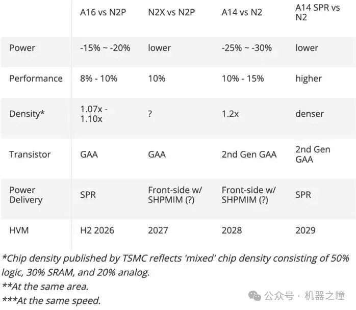
TSMC originally planned to use 2 nanometer process for the Baoshan fab 20 plant, with the second plant being converted to 1.4 nanometer process and R&D line, the third plant for 1 nanometer process and R&D line, and the fourth plant not ruling out 0.7 nanometer process and R&D line. The Central Science Park’s preliminary plan includes four factories, with the first phase consisting of two factories for 1.4 nanometer process, and the second phase potentially including two factories for 1 nanometer process. Additionally, TSMC has planned to invest in the Nanshalun area to establish a 1 nanometer advanced process base, with the current land area reaching 500 hectares, which is estimated to accommodate 10 wafer fabs.