Gobi Jia is laying out glass substrates, and nano-microcrystalline glass has entered the terminal supply chain

Microcrystalline glass: Source:Gobi Jia
On June 12, during the 2025 online collective reception day for investors of listed companies in Hubei, the person in charge of Gobi Jia stated that the company’s glass substrate and carrier board business has just started, with some material research and development in the pilot stage. In the past year of strategic advancement, the company has established a complete R&D system and achieved significant results in the field of special functional glass materials, with nano-microcrystalline glass products successfully entering the supply chain of some terminal customers. In the future, Gobi Jia will continue to increase R&D investment in the application field of semiconductor glass substrates and actively expand market space.
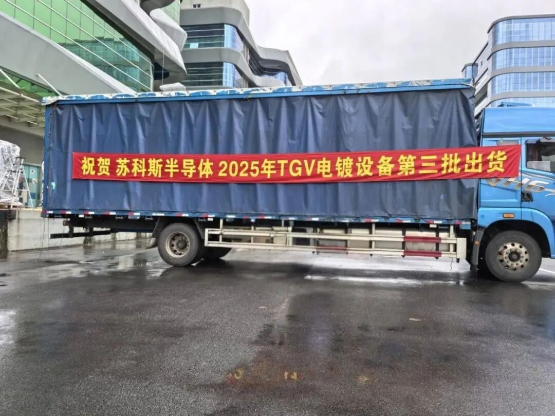
SuKeSi has completed the shipment of the third batch of glass through-hole (TGV) electroplating equipment, continuing to lead the innovation in advanced packaging technology
Source: SuKeSi
SuKeSi Semiconductor, following two successful deliveries, has once again reached an important milestone—the third batch of TGV electroplating equipment was successfully shipped on June 13, 2025, to the customer’s location. This milestone event marks the increasing maturity of SuKeSi Semiconductor’s R&D, production, quality control, and supply chain systems in the TGV field, further consolidating and enhancing delivery capabilities.
YunTian Semiconductor’s 3D Glass IPD mass production project has delivered over ten million units
In Q2 2025, the 3D Glass IPD mass production project designed by Shanghai Chipwave and manufactured by YunTian Semiconductor has delivered over ten million units, marking the stable mass production of the world’s first 3D Glass IPD production line, injecting strong “core” power into fields such as AI, automotive electronics, and IoT applications.
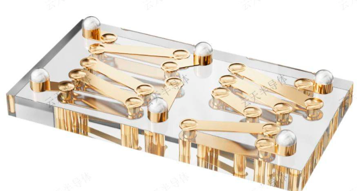
3D IPD structure diagram Source: YunTian Semiconductor
YunTian Semiconductor uses glass as a substrate, employing unique and stable 2.5D TGV metal interconnect technology and high-precision wiring layer processes to produce high-performance IPD devices, which exhibit excellent comprehensive performance in terms of device size, Q value, insertion loss, and out-of-band suppression.
Display panel leader BOE is advancing its semiconductor glass substrate business
Source: BOE
Public bidding information released on June 18 shows that BOE has recently placed an order for a batch of semiconductor glass substrate production equipment, including automatic optical inspection (AOI) equipment and electroless copper plating equipment.
In the bidding documents, BOE explained that the procurement of these glass substrate process equipment, exposure equipment, etc., is to establish a research and development and industrialization testing line based on glass substrate packaging process technology. The goal is to verify the process technology of glass substrate integrated circuit packaging substrates and achieve industrialization, thereby enhancing chip performance and enabling large-size packaging. This clearly indicates that this batch of equipment is not for producing display screens but for semiconductor packaging.
Samsung is focusing on the next generation of semiconductor packaging technology: glass substrates and glass interlayers
Source: Samsung
Korean media reports indicate that Samsung Electronics’ Device Solutions Division is accelerating the development of the next generation of chip packaging materials, “glass interlayers,” aimed at replacing expensive silicon interlayers and enhancing chip performance.
Compared to silicon interlayers, glass interlayers not only have lower costs but also possess heat resistance and impact resistance characteristics, making microcircuit processing more convenient and less prone to bending during large-size packaging, which is a key technology for enhancing semiconductor competitiveness.
Samsung plans to achieve mass production of glass interlayers by 2027, which aligns with the mass production schedule of its subsidiary Samsung Electro-Mechanics for glass substrates. Currently, Samsung has partnered with material suppliers Chemtronics and equipment manufacturers Philoptics to conduct research and development based on Corning glass.
Reference sources:
Various company websites

Video Recommendations

Note: Images are for non-commercial use; infringement notifications will be deleted! To join the powder industry exchange group, please add the WeChat of the China Powder Network editorial department: 18553902686
Click the “Read Original” button below to register for the conference↓↓↓