Core Innovation Summary
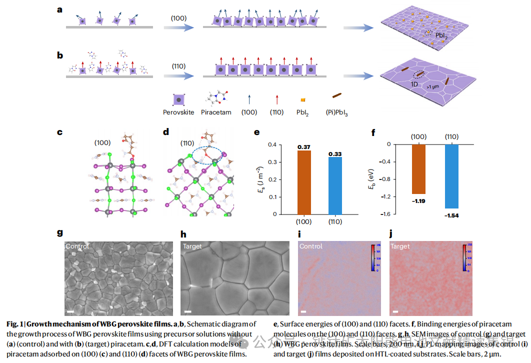
Innovation: By introducing Piracetam as a crystal modifier, we optimize the nucleation and grain boundary structure of wide bandgap perovskite (WBG, 1.77 eV), achieving large grain sizes (1 μm), preferred orientation ((110) crystal plane), and one-dimensional needle-like structures (1D (Pi)PbI₃), significantly enhancing device efficiency and stability.
Implementation Method:
Molecular Regulation: Piracetam binds with uncoordinated Pb²⁺ through amide groups, inhibiting defect formation and preferentially adsorbing on the (110) crystal plane, promoting uniform crystallization.
Post-Treatment Reaction: During the annealing process, Piracetam reacts with residual PbI₂ to generate one-dimensional nanoneedles at the grain boundaries, passivating defects and inhibiting ionic migration.
Effects:
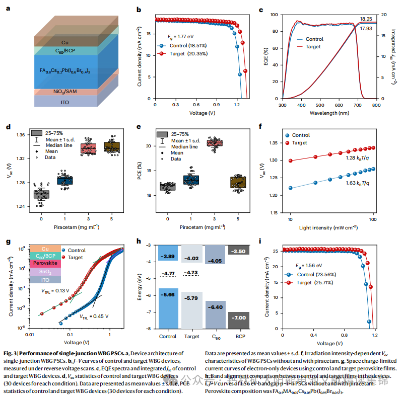
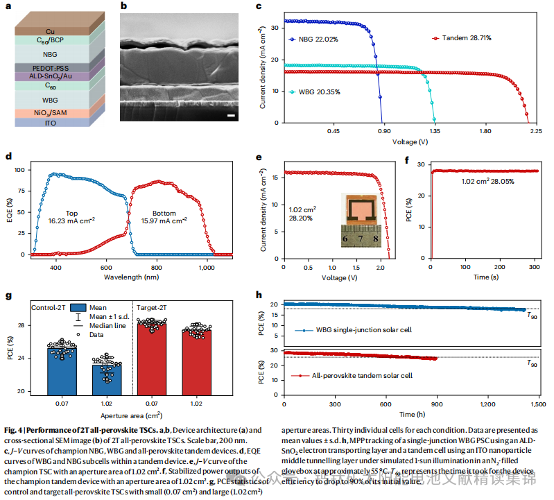
Efficiency Improvement: The efficiency of single-junction WBG devices reaches 20.35% (certified VOC=1.36 V), while the efficiencies of all-perovskite tandem devices (0.07 cm² and 1.02 cm²) are 28.71% and 28.20%, respectively, with the efficiency difference between small and large area devices reduced to 0.51%.
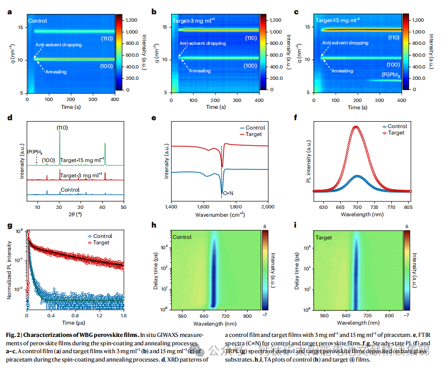
Scalability Compatibility: The surface roughness of WBG perovskite films is reduced to 17.2 nm (compared to 28.6 nm in the control group), making it suitable for large-area coating techniques (such as blade coating).
Author Team: Jointly published by Ke Weijun from Wuhan University, South China Normal University, and Shanghai Synchrotron Radiation Facility.
Perovskite Component Device Structure
1. Single-junction wide bandgap (WBG) device (1.77 eV):
Transparent Electrode: ITO (Indium Tin Oxide).
Hole Transport Layer (HTL): NiOx nanoparticles + Me-4PACz (self-assembled monolayer).
Perovskite Absorbing Layer: FA0.8Cs0.2PbI1.8Br1.2 (with Piracetam added).
Electron Transport Layer (ETL): C60 (fullerene) + BCP (bathocuproine).
Top Electrode: Thermal evaporation of Cu (100 nm).
2. All-perovskite tandem device (WBG + NBG):
Top WBG sub-cell: Same as above.
Intermediate Composite Layer: ALD-SnO₂ + ultrathin Au (1 nm) + PEDOT:PSS.
Bottom Narrow Bandgap (NBG) sub-cell: FA0.7MA0.3Sn0.5Pb0.5I₃ (with AspCl passivation agent added).
Top Electrode: C60 + BCP + Cu.
Solution Preparation and Device Fabrication Process
1. WBG perovskite precursor solution:
Formula: Dissolve FAI, PbI₂, PbBr₂, CsI in a stoichiometric ratio in a mixed solvent of DMF:DMSO (4:1), concentration 1.2 M.
Additive: Piracetam (3–15 mg/ml) is directly added to the precursor solution.
2. Single-junction WBG device fabrication::
Substrate Treatment: ITO glass is ultrasonically cleaned (water → acetone → isopropanol → ethanol) and plasma cleaned.
HTL deposition:
NiOx nanoparticle solution (10 mg/ml aqueous solution) is spin-coated (3000 rpm, 35 s), followed by annealing at 140°C for 30 minutes.
Me-4PACz solution (0.3 mg/ml ethanol) is spin-coated (3000 rpm, 30 s), followed by annealing at 100°C for 10 minutes.
Perovskite Spin Coating:
Precursor solution (40 μl) is dropped, first spinning at 1000 rpm for 5 seconds, then at 5000 rpm for 30 seconds, while adding ether anti-solvent (300 μl).
Annealing: 65°C for 2 minutes → 100°C for 15 minutes.
Surface Passivation: PDAI₂ solution (2 mg/ml isopropanol) is spin-coated (4000 rpm, 30 s), followed by annealing at 100°C for 10 minutes.
Top Electrode Deposition: Sequentially deposit C60 (20 nm), BCP (7 nm), Cu (100 nm).
3. All-perovskite tandem device fabrication:
WBG sub-cell: After depositing the C60 layer, deposit ALD-SnO₂ (20 nm).
Intermediate Composite Layer: Deposit 1 nm Au, spin-coat PEDOT:PSS (5000 rpm, 30 s), followed by annealing at 100°C for 15 minutes.
NBG sub-cell:
Precursor solution (FA0.7MA0.3Sn0.5Pb0.5I₃, 2.1 M) is spin-coated (1000→4000 rpm), followed by annealing at 100°C for 10 minutes.
Passivation: AspCl solution (0.2 mg/ml isopropanol) is spin-coated (4000 rpm, 30 s), followed by annealing at 100°C for 7 minutes.
Top Electrode: Deposit C60, BCP, Cu.
Original Link: https://www.nature.com/articles/s41560-025-01760-6#Sec17
If there are any misunderstandings or copyright issues, please contact for removal.