1. Introduction
Recently, I have developed an interest in Two-Wire CJTAG. This article mainly records some of my insights on Two-Wire CJTAG. There are many debugging interfaces, with SWD and JTAG being the most commonly used. For articles related to SWD and JTAG on this public account, you can refer to this series – “Making a Debugger Based on the Xianji Microcontroller“
Two-Wire CJTAG is part of IEEE 11497.7-2022 (the 2022 version of IEEE obtained for this article). The emphasis on Two-Wire is important because in IEEE 11497.7, CJTAG includes both two-wire and four-wire modes. This article mainly elaborates on Two-Wire CJTAG (TMSC and TCK), with the data format being OScan1.
There is very little description online regarding Two-Wire CJTAG; the only resource available is the Segger wiki on how to use CJTAG to connect to target devices. For example, the connection can be found here: https://kb.segger.com/J-Link_cJTAG_specifics.
The IEEE 11497.7 standard is over 1000 pages long, which is quite cumbersome compared to the 100 pages of IEEE 11497.1 (JTAG), making it equally difficult to read.
By the way, when using AI, one must be able to discern clearly, as AI can easily make mistakes when online resources are not abundant, leading to self-justifying explanations. For example, when asking ChatGPT about the full name of CJTAG’s TAP.7 OAC, the explanation was as follows:
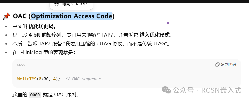
However, the standard description in IEEE 11497.7 states: OAC stands for online activation code.
This article mainly analyzes the waveforms of the two connection sequences of CJTAG used with Jlink, in conjunction with the IEEE 11497.7 documentation, to interpret its instructions.
2. CJTAG Connection Sequences
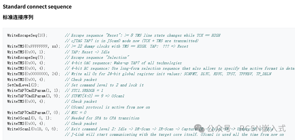
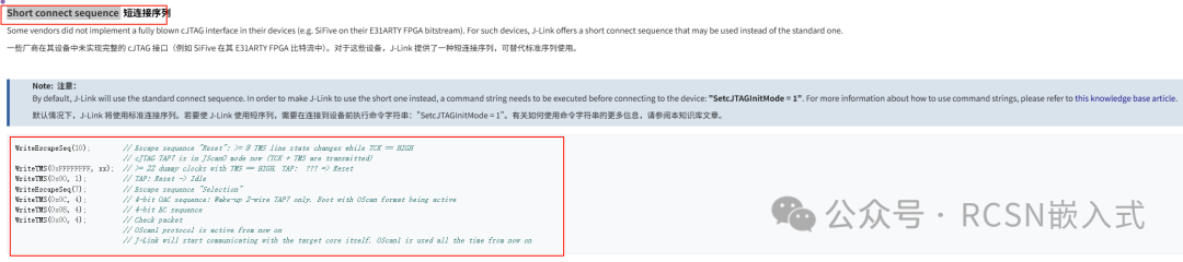
Before using CJTAG to access related registers, the debugger needs to ensure that the target device’s CJTAG interface is in a defined mode, such as Two-Wire TMS+TCK, with the data format being OScan1. In Jlink, there are two connection sequences: Standard connect sequence and Short connect sequence.
(1) Reset Operation of TAP.7 and TAP.1 Controllers
(1) Escape Detection Function of TAP.7 Controller
The interface of WriteEscapeSeq mentioned above performs the escape function, which is explained in the IEEE standard as follows:
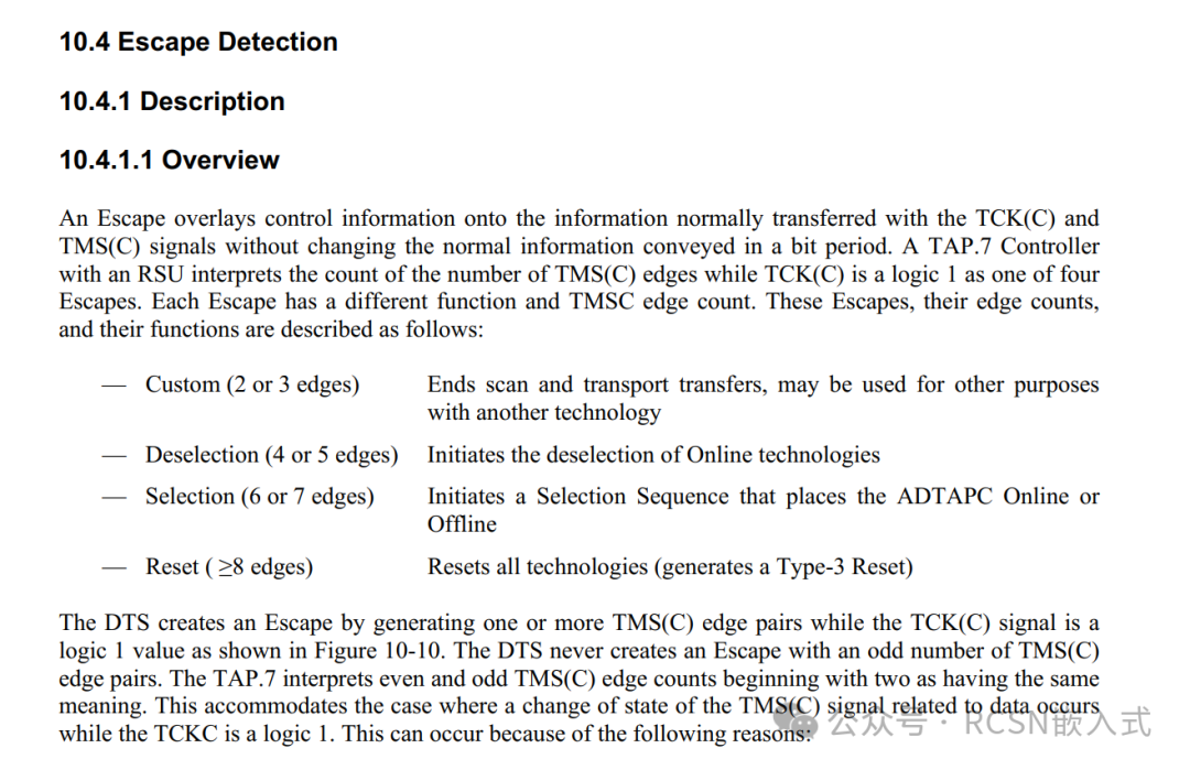
Without altering the normal information transmitted by TCK(C) and TMS(C) signals within a bit period, control information is superimposed onto these signals. The TAP.7 controller interprets the edge counts of the TMS(C) signal when TCK(C) is logic 1 as one of four different escapes. Each escape corresponds to different functions and TMSC edge counts. Specifically:
— Custom (2 or 3 edges): Ends scanning and transmission operations, and can also be combined with other techniques for other purposes.
— Deselection (4 or 5 edges): Initiates deselection of online technology.
— Selection (6 or 7 edges): Initiates selection sequence, setting ADTAPC to online or offline.
— Reset (8 or more edges): Resets all technologies (producing Type-3 reset).
This means that when TCK is high, if TMS continuously toggles and there are enough toggles, the TAP.7 controller considers it has entered escape mode.
Corresponding IEEE standard screenshot:
It also lists the timing:
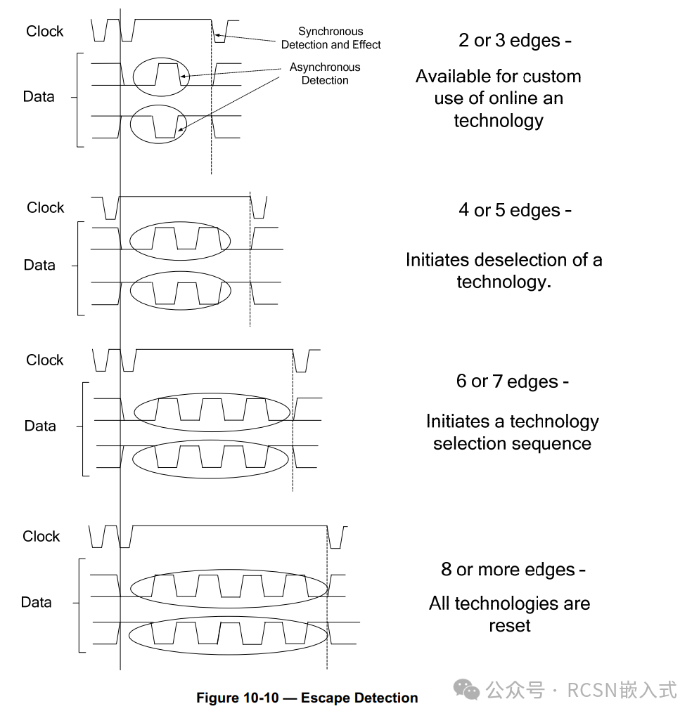
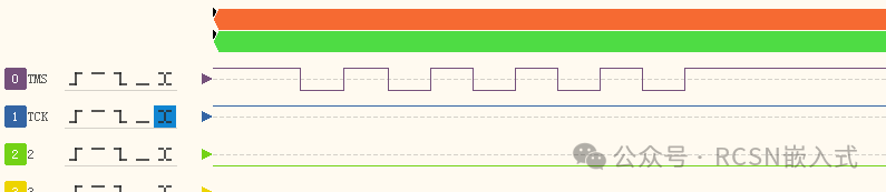
From the above, it can be seen that in the Jlink CJTAG connection sequence, whether it is a standard or short connection, the initial WriteEscapeSeq(10); resets the TAP.7 controller, with the reset requirement being that TCK remains high and TMS toggles continuously more than 8 times.
The captured waveform also shows that Jlink sent TMS with 10 continuous toggles.
For WriteTMS(0xFFFFFFFF, xx); and WriteTMS(0x00, 1); these are for resetting the TAP.1 state machine and entering IDLE.
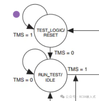
In the Jlink waveform, it can also be seen that during the sustained period of TCK, TMS is high, ensuring that TAP.1 enters RESET, and in the last TCK period, TMS becomes 0, indicating it has entered IDLE.
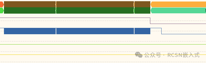
Therefore,
WriteEscapeSeq(10);
WriteTMS(0xFFFFFFFF, xx);
WriteTMS(0x00, 1);
These actually reset TAP.7 and TAP.1, ensuring that the controllers enter their initial states.
(2) Selection Sequence of TAP.7 Controller
From the above escape function, it can be seen that when TCK=1, TMS toggles continuously 6 to 7 times, the selection sequence is initiated. This selection sequence is actually used to configure some register operations of the TAP.7 controller, such as setting the CJTAG format data to OScan1.
In the standard connection sequence of Jlink, this is implemented as follows:
WriteEscapeSeq(7);         // Escape sequence "Selection"
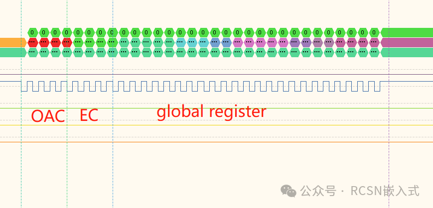
WriteTMS(0x00, 4);         // 4-bit OAC sequence: Wake-up TAP7 of all technologies
WriteTMS(0x00, 4);         // 4-bit EC sequence: Use long-form selection sequence that also allows to specify the active format in detail
WriteTMS(0x00000000, 24);  // Write all 0s for 24-bit global register init values: SCNFMT, DLYC, RDYC, TPST, TPPREV, TP_DELN
WriteTMS(0x00, 4);         // Check packet
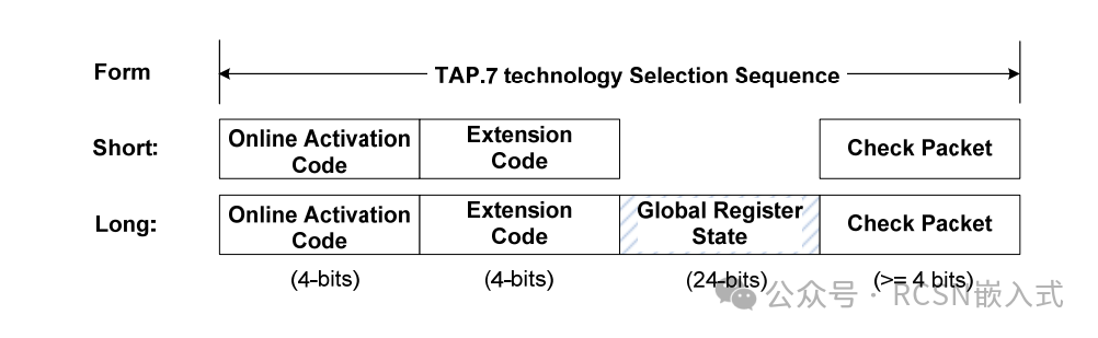
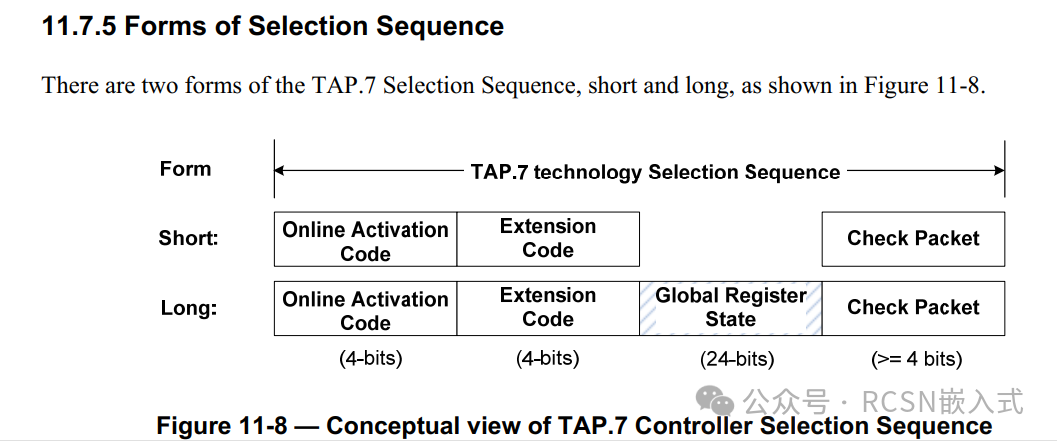
In IEEE 11497.7, the selection sequence is divided into short and long sequences, as shown in the figure:
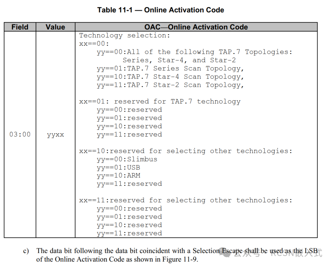
The meanings of the 4-bit online activation code (OAC) are as follows:
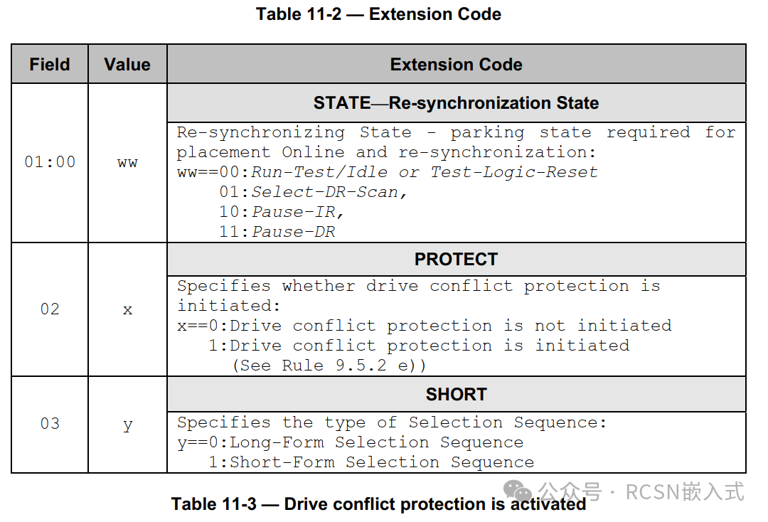
The meanings of the 4-bit extension code (EC) are as follows:
Global Register load (24-bit)
When the SHORT bit in the extension code is logic 0, the long form of the TAP.7 selection sequence is used. Otherwise, the short selection sequence will be used. Using the long format selection sequence specifies the TAP.7 controller global register configuration required for standard and advanced protocol features as a shift register, as shown in Figure 11-11.
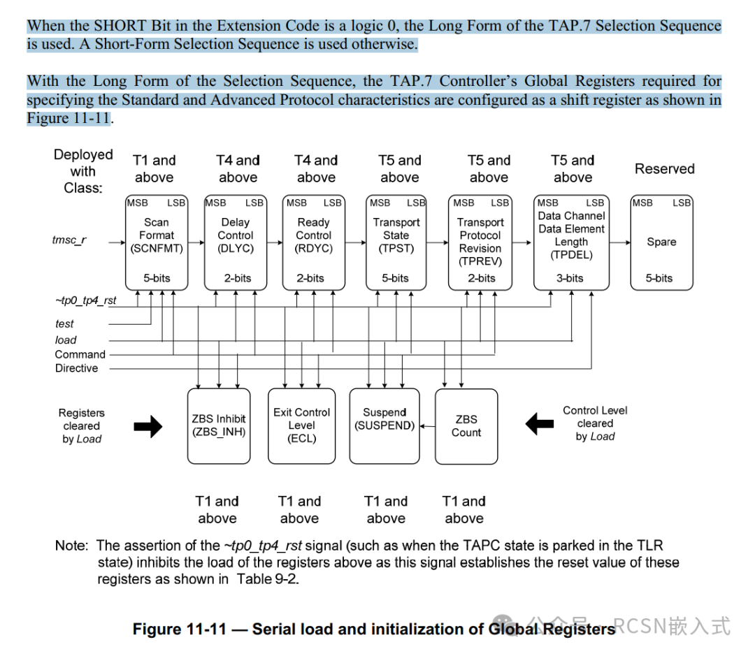
From this, it can be understood that if a standard sequence connection is to be selected, the relevant commands to operate the TAP controller need to be executed in both standard and advanced commands. If the SHORT bit of the EC is 0, then it can be implemented in a short connection, but the set of commands for this implementation is limited.
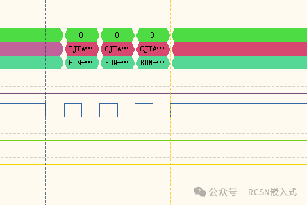
Let’s take a look at the timing diagram of the selection sequence:
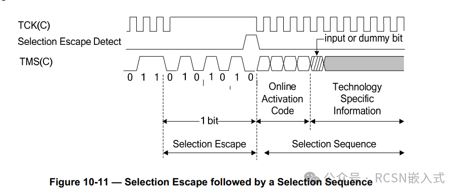
It can be seen that WriteEscapeSeq(7); is the entry into selection escape.
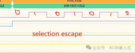
WriteTMS(0x00, 4)
WriteTMS(0x00, 4);
WriteTMS(0x00000000, 24);
These correspond to OAC + EC + global reg.
Finally, there is also Check packet WriteTMS(0x00, 4);
(3) Commands of TAP.7 Controller

TAP.7 commands are implemented using only TCK(C) and TMS(C) signals. This means that the standard protocol can manage TAP.7 controller functions independently of the availability of TDI and TDO signals.
In the standard connection sequence of Jlink, this involves operating the relevant command registers of the controller.
SetCmdLevel(2);            // Set command level to 2 and lock it
WriteTAP7Cmd1Param(1, 1);  // STC1.SREDGE = 1
WriteTAP7Cmd1Param(3, 9);  // STFMT[4:0] == 9 => OScan1
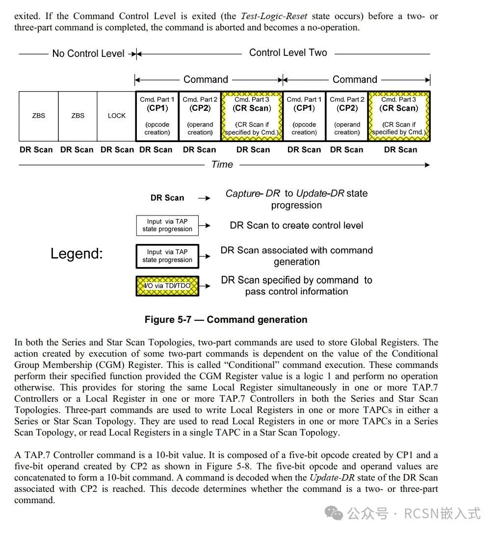
The corresponding standards are divided into ZBS + LOCK + command. Here, I will explain these abbreviations one by one.
(1) ZBS (Zero-bit DR Scans)
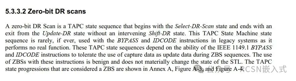
Zero-bit DR Scan (ZBS) is a TAPC state sequence that starts from the Select-DR-Scan state and ends without going through the Shift-DR state, exiting from the Update-DR state.
Starting from ZBS count = 0, each time a ZBS occurs consecutively, the ZBS counter increments by one, with a maximum of 7.
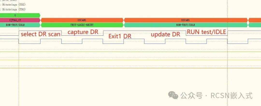
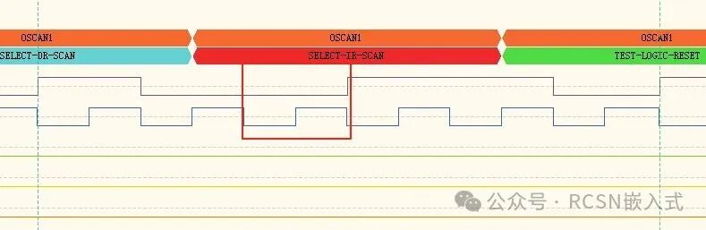
From the Jlink waveform, it can be seen that a ZBS looks like this. It can be seen that the entire sequence did not go through the shift DR state, which is zero bit DR scans.
(2) Lock ZBS (Locking ZBS Count)
When a DR scan that includes the Shift-DR state occurs and the ZBS count is greater than zero, the ZBS count will be locked at its current value.
Once the ZBS count is locked, subsequent ZBS occurrences will not change the locked value.
Locking the ZBS count is equivalent to “storing the count value for later use”.
From the waveform, it can be seen that lock ZBS has an additional shift DR scan.
(3) Control Levels
The corresponding control levels are achieved through the ZBS count, just like the aforementioned SetCmdLevel(2);
The generation of control levels starts from No control level and EPU running state = RUNNING (EPU state see 5.3.3.4).
The EPU running state determines whether ZBS is recognized and whether it is used by the TAP.7 controller for functional operations.
When ZBS is locked, if it is used by the TAP.7 controller to perform controller functions, a control level will be activated, with the level value equal to the locked ZBS count (1–7). Otherwise, it is merely a locked count.
The different control levels correspond to the following functions (with levels in parentheses):
(1) ZBS can be used by STL or other functions(2) TAP.7 command generation(3) Reserved(4–5) Access optional TAP.7 controller scan paths(6) Force offline operation (optional)(7) DTS usage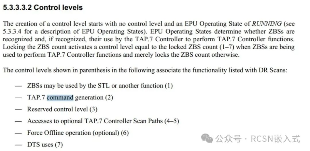
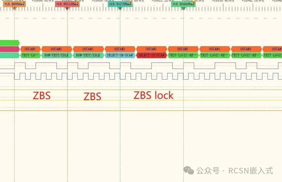
From Jlink, it can be seen that there were two occurrences of ZBS, and the last occurrence of ZBS lock indicates that it has entered control level 2.
(4) Commands
We will analyze from WriteTAP7Cmd1Param(3, 9); // STFMT[4:0] == 9 => OScan1.
From the IEEE standard, it can be seen that 3 represents the store of STFMT.
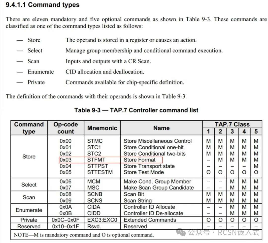
The corresponding SCNFMT of 9 is the data format of OScan1.
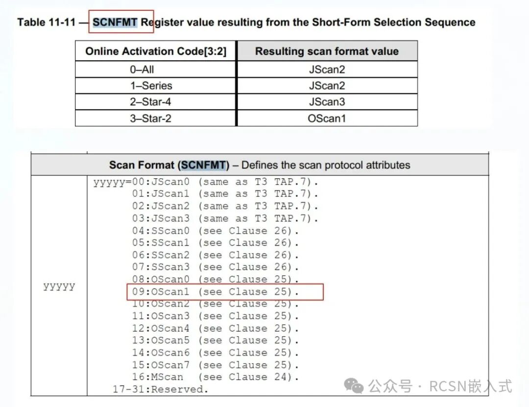
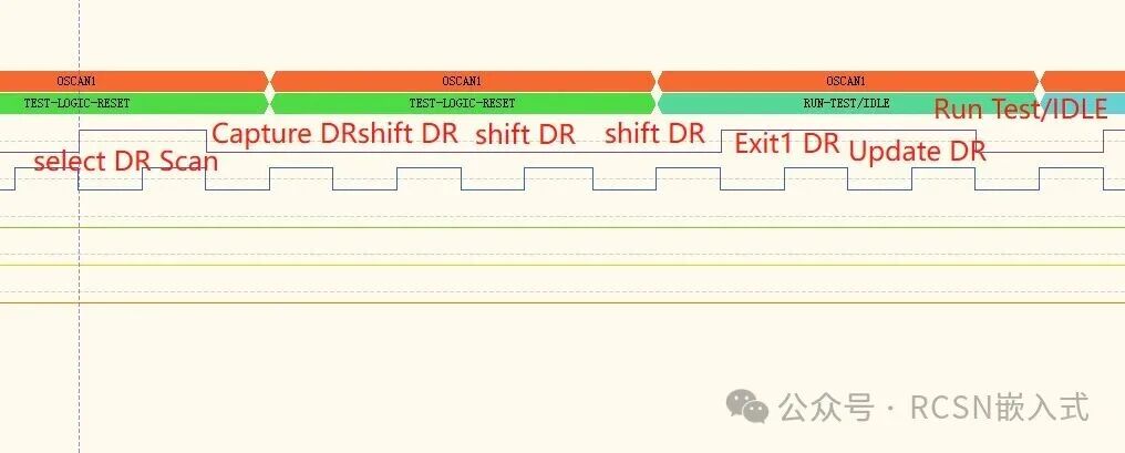
Since TDI and TDO are disabled during the TAP.7 command phase, data shifting is performed through TMS operations to shift DR. The number of shifts corresponds to the number of shift DR operations.
Now, looking at the waveform for CP1 being 3: it can be seen that shift DR occurred three times, indicating that it has shifted 3 times, making CP1 equal to 3.
3. Conclusion
Through the analysis of the Two-Wire CJTAG connection sequence waveforms of Jlink, combined with the IEEE 11497.7-2022 standard, we can see:
1. Reset Mechanism
Through WriteEscapeSeq(10), utilizing the rule of TCK high level with TMS toggling more than 8 times, the reset of the TAP.7 controller is completed.WriteTMS(0xFFFFFFFF,xx) and WriteTMS(0x00, 1) ensure that the TAP.1 state machine is reset and enters IDLE.Thus, both TAP.7 and TAP.1 are guaranteed to be in their initial, controllable states.
2. Selection Sequence
Utilizing WriteEscapeSeq(7) triggers the selection sequence, entering the configuration process of OAC (Online Activation Code) + EC (Extension Code) + Global Register.Where OAC/EC determines the type of selection sequence (long or short), and the Global Register is used to load the TAP.7 global register configuration.For example, the long sequence form implemented in the Jlink waveform allows for clear setting of data formats (such as OScan1).
3. TAP.7 Command Mechanism
Through ZBS (Zero-bit DR Scan) and ZBS lock, the switching of control levels is completed.The control level determines whether TAP.7 enters command mode and whether it can execute related register writes.At control level 2, through WriteTAP7Cmd1Param(3, 9), the STFMT is set to 9, which corresponds to the OScan1 format.It is worth noting that during the TAP.7 command phase, TDI/TDO are disabled, and shifting operations rely entirely on TMS’s shift-DR.
This article focuses on the interface connection of CJTAG and the control process of TAP.7. The specific methods for accessing the target chip’s IR/DR and internal functions using the OScan1 format will be elaborated in subsequent articles.
Combining the verification of Jlink’s waveforms, one can intuitively understand the tedious protocol descriptions in IEEE 11497.7, which is of certain reference value for subsequent research on self-developed debuggers or chip debugging interface design.