
The motor driver IC transmits a large amount of current while also dissipating a significant amount of electrical energy. Typically, the energy is dissipated into the copper areas of the printed circuit board (PCB). To ensure sufficient cooling of the PCB, special PCB design techniques must be employed. In this first part of the article, we will provide some general recommendations for PCB design of motor driver ICs.Use Large Copper Areas!
Copper is an excellent conductor of heat. Since the substrate material of the PCB (FR-4 glass epoxy resin) is a poor conductor of heat, from a thermal management perspective, the more copper area on the PCB, the better the heat conduction.
A thick copper plate of 2 ounces (68 microns thick) has better thermal conductivity compared to a thinner copper plate. However, thick copper is not only expensive but also difficult to achieve fine geometries. Therefore, a 1-ounce (34 microns thick) copper plate is usually selected. The outer layers often use 1/2 ounce of copper plating, with a thickness of up to 1 ounce.
In multilayer boards, internal layers often use solid copper plates for better heat dissipation. However, since their planar layers are typically located in the center of the circuit board stack, heat may be trapped inside the circuit board. Thus, copper areas can be added to the outer layers of the PCB, connecting to the internal layers through vias to transfer heat out.
Due to traces and components present in double-sided PCBs, heat dissipation becomes more challenging. Therefore, motor driver ICs should use as much solid copper and thermally conductive vias as possible. Casting copper on both sides of the outer layer and connecting them with vias can help disperse heat to different areas separated by traces and components.
Traces Must Be Wide—The Wider, The Better!
Since the current flowing through the motor driver IC can be significant (sometimes exceeding 10A), careful consideration should be given to the PCB trace width connecting to the chip. The wider the trace, the lower the resistance. The trace width must be adjusted to ensure that the resistance in the trace does not cause excessive energy dissipation, leading to increased trace temperature. However, traces that are too thin can easily burn out like a fuse.
Designers typically use the IPC-2221 standard to calculate the appropriate trace thickness. This specification includes a chart showing the copper cross-sectional area and allowable temperature rise for different current levels, allowing for the conversion of trace width based on a given copper layer thickness. For example, a trace width of exactly 7mm is required to carry a 10A current with a temperature rise of 10°C in a 1-ounce thick copper layer, while only 0.3mm is needed for a 1A current.
According to this method, it seems impossible to run a 10A current through a micro IC pad.
Thus, it is important to understand the IPC-2221 standard’s recommendations for trace widths for long PCB traces. If the trace connects to a larger trace or copper area, using a short segment of PCB trace to carry a larger current does not have adverse effects. This is because the resistance of a short and narrow PCB trace is very low, and the heat generated is absorbed into the wider copper area. As shown in Figure 1, even if the thermal pad in this device is only 0.4mm wide, it can carry up to 3A of continuous current because the trace width has been increased as close to the actual width of the device as possible.
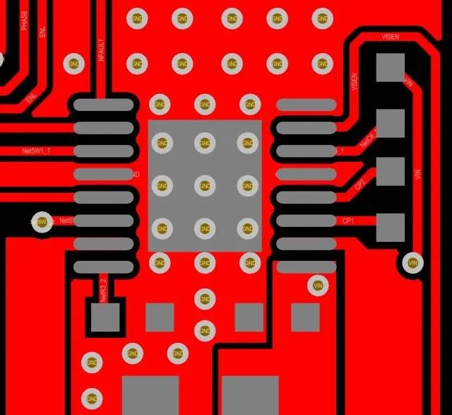
Figure 1: Widening PCB TracesSince the heat generated by narrower traces can conduct to wider copper areas, the temperature rise of narrow traces can be negligible.Traces embedded in the internal layers of the PCB do not dissipate heat as effectively as outer layer traces because the insulating material has poor thermal conductivity. Therefore, the width of internal traces should be twice that of external traces.Table 1 provides a rough recommendation for the width of long traces (greater than 2cm) in motor driver applications.
| Current(RMS or DC) | Trace Width for 1 Ounce Copper | Trace Width for 2 Ounce Copper | ||
| Outer Layer | Inner Layer | Outer Layer | Inner Layer | |
| ≤1A | 0.6mm | 1.2mm | 0.3mm | 0.6mm |
| 2.5A | 1mm | 2mm | 0.5mm | 1mm |
| 5A | 2.5mm | 5mm | 1.2mm | 2.5mm |
| 10A | 7mm | 14mm | 3.5mm | 7mm |
Table 1: PCB Trace WidthIf space allows, the wider the traces or copper pours, the more the temperature rise can be minimized, and the voltage drop can be reduced.Thermal Vias—The More, The Better!Vias are small plated holes typically used to transfer signal traces from one layer to another. As the name implies, thermal vias transfer heat from one layer to another. Proper use of thermal vias can effectively help PCB heat dissipation, but many practical production issues also need to be considered.Vias have thermal resistance, which means that whenever heat flows through, there will be a certain temperature difference across the vias, measured in degrees Celsius per watt. Therefore, to minimize thermal resistance and improve the heat dissipation efficiency of vias, they should be designed larger, and the copper area inside the vias should be as large as possible (see Figure 2).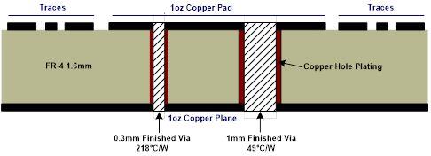 Figure 2: Cross-section of a ViaWhile larger vias can be used in open areas of the PCB, vias are often placed inside thermal pads to directly dissipate heat from the IC package. In this case, it is not possible to use large vias, as overly large plated vias can lead to “solder wicking,” where the solder used to connect the IC to the PCB flows into the vias, resulting in poor solder joints.There are several methods to reduce “solder wicking.” One is to use very small vias to minimize the solder that can enter the vias. However, the smaller the via, the higher the thermal resistance, so more small vias are needed to achieve the same heat dissipation performance.Another technique is to “cover” the vias on the back of the PCB. This requires removing the opening of the solder mask layer on the back, allowing the solder mask material to cover the vias. The solder mask will cover small vias so that solder cannot wick into the PCB.However, this brings another issue: flux retention. If the solder mask layer covers the vias, flux may remain inside the vias. Some flux formulations are corrosive, and if not removed for an extended period, they can affect the reliability of the chip. Fortunately, most modern no-clean flux processes are non-corrosive and will not cause issues.It is important to note that thermal vias themselves do not have cooling functions; they must be directly connected to copper areas (see Figure 3).

Figure 3: Thermal ViasIt is recommended that PCB designers consult with the SMT process engineers at the PCB assembly factory to determine the best via sizes and constructions, especially when vias are located inside thermal pads.Soldering Thermal PadsIn TSSOP and QFN packages, the bottom of the chip is soldered to large thermal pads. These pads connect directly to the back of the die for device heat dissipation. The pads must be well soldered to the PCB to dissipate power.IC datasheets do not always specify the paste opening for the pads. Typically, SMT process engineers have their own set of rules regarding how much solder to place and what shape the via molds should take.If the opening is the same size as the pad, more solder will be required. When the solder melts, its tension will cause the device surface to bulge. Additionally, it can lead to solder voids (cavities or gaps within the solder). Solder voids occur when volatile substances in the flux evaporate or boil during the solder reflow process, causing solder to separate at the joint.To address these issues, for pads larger than approximately 2mm², solder paste is typically deposited in several smaller square or circular areas (see Figure 4). Distributing the solder across multiple smaller areas allows the volatile substances in the flux to evaporate more easily, preventing solder separation.
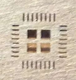
Figure 4: QFN SolderingAgain, it is recommended that PCB designers work with SMT process engineers to collaboratively determine the correct solder pad mold openings. Online papers can also be referenced.Component PlacementThe component placement guidelines for motor driver ICs are similar to those for other power ICs. Bypass capacitors should be placed as close to the device power pins as possible, with large capacitance capacitors placed nearby. Many motor driver ICs will use bootstrap capacitors or charge pump capacitors, which should also be located near the IC.Please refer to the component placement example in Figure 5. Figure 5 shows the dual-layer PCB layout for the MP6600 stepper motor driver. Most signal traces are directly arranged on the top layer. The power traces loop from the large capacitance capacitor to the bypass, using multiple vias on the bottom layer to switch layers.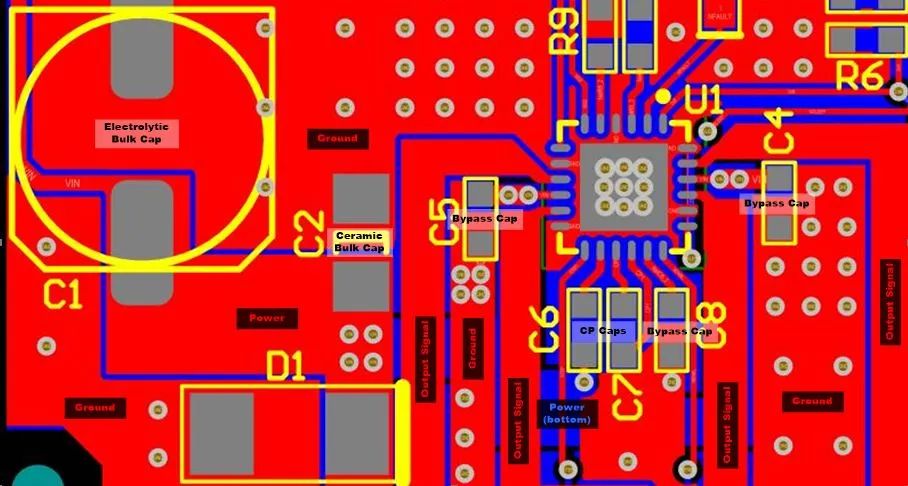 Figure 5: MP6600 Component PlacementIn the next part of this article, we will explore detailed packaging methods and PCB layout for motor driver ICs.
Next Part
In the first part of this article, we provided some general recommendations for PCB layout to achieve proper performance for motor driver ICs. In the next part, we will offer specific PCB layout recommendations for using typical packages of motor drivers.
Lead Package Layout
Standard lead packages (such as SOIC and SOT-23 packages) are typically used in low-power motor drivers (Figure 6).
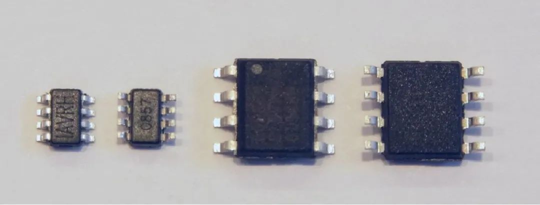 Figure 6: SOT 23 and SOIC PackagesTo fully enhance the power dissipation capability of lead packages, MPS employs a “flip-chip lead frame” structure (Figure 7). Without using bonding wires, copper bumps and solder are used to attach the chip to the metal leads, allowing heat to be conducted from the chip to the PCB through the leads.
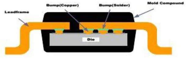 Figure 7: Flip-Chip Lead FrameBy connecting larger copper areas to leads carrying larger currents, thermal performance can be optimized. On motor driver ICs, the power, ground, and output pins are typically connected to copper areas.
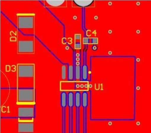 Figure 8: Flip-Chip SOIC PCB LayoutFigure 8 shows a typical PCB layout for the “flip-chip lead frame” SOIC package. Pin 2 is the device power pin. Note that the copper area is located near the top layer device, with several thermal vias connecting this area to the copper layer on the back of the PCB. Pin 4 is the ground pin, connected to the surface layer ground copper area. Pin 3 (device output) is also routed to a larger copper area.
QFN and TSSOP Packages
The TSSOP package is rectangular and uses two rows of pins. The TSSOP package for motor driver ICs typically has a large exposed pad on the bottom for dissipating heat from the device (Figure 9).
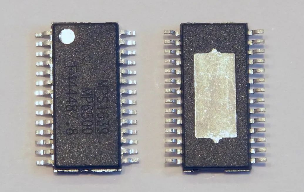 Figure 9: TSSOP PackageThe QFN package is a leadless package with a pad around the outer edge of the device, and a larger pad in the center of the bottom for absorbing heat from the chip (Figure 10).
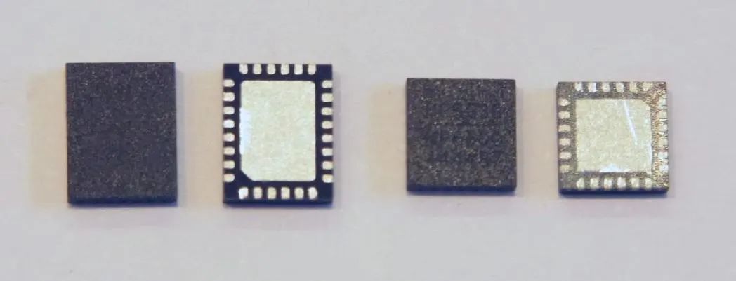 Figure 10: QFN PackageTo dissipate heat from these packages, the exposed pads must be well soldered. The exposed pads are usually at ground potential, allowing them to connect to the PCB ground layer. In the example of the TSSOP package shown in Figure 11, an array of 18 vias with a drilling diameter of 0.38 mm is used. The calculated thermal resistance for this via array is approximately 7.7°C/W.
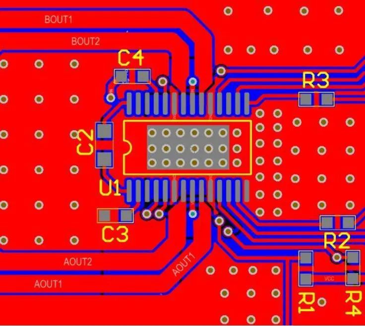 Figure 11: TSSOP PCB LayoutTypically, these thermal vias use drilling diameters of 0.4 mm or smaller to prevent solder wicking. If the SMT process requires smaller diameters, the number of vias should be increased to maintain a low overall thermal resistance.In addition to vias located in the pad area, thermal vias are also present in the outer area of the IC. In TSSOP packages, copper areas can extend beyond the ends of the package, providing another route for heat to escape through the top copper layer.The pads surrounding the edges of the QFN package should avoid using copper layers on the top to absorb heat. Thermal vias must be used to dissipate heat to the inner layer or the bottom layer of the PCB.The PCB layout shown in Figure 12 is for a small QFN (4 × 4 mm) device. In the exposed pad area, only nine thermal vias are accommodated (see Figure 12). Therefore, the thermal performance of this PCB is not as good as that of the TSSOP package shown in Figure 11.
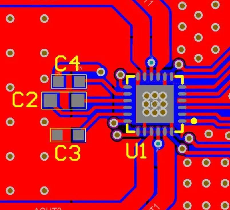 Figure 12: QFN (4mmx4mm) Layout
Flip-Chip QFN Package
The flip-chip QFN (FCQFN) package is similar to the conventional QFN package, but the chip is connected directly to the board at the bottom of the device in a flip-chip manner instead of connecting to the package board using bonding wires. These boards can be placed on the backside of power devices on the chip, so they are typically arranged in long strips rather than small pads (see Figure 13).
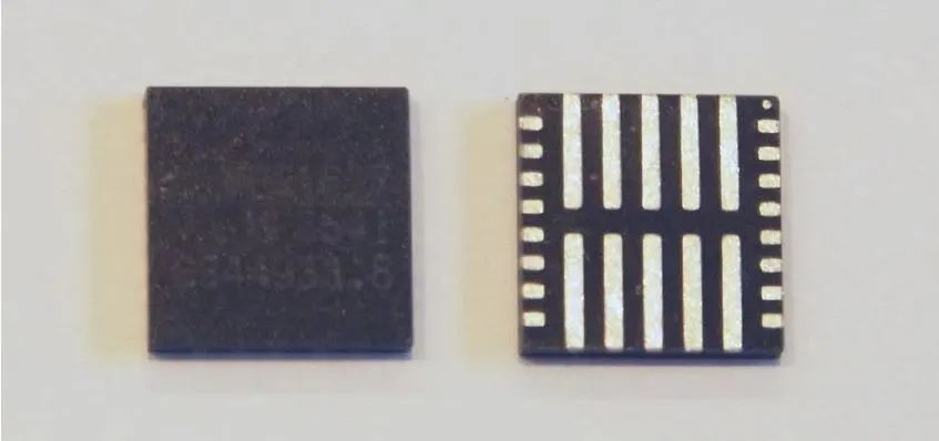
Figure 13: FCQFN PackageThis package uses multiple rows of copper bumps on the surface of the chip to connect to the lead frame (Figure 14).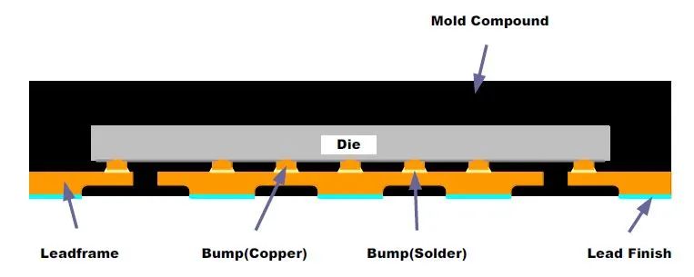 Figure 14: FCQFN StructureSmall vias can be placed within the pad area, similar to conventional QFN packages. On multilayer boards with power and ground layers, vias can directly connect these boards to each layer. In other cases, copper areas must be directly connected to the board to absorb heat from the IC into larger copper areas.
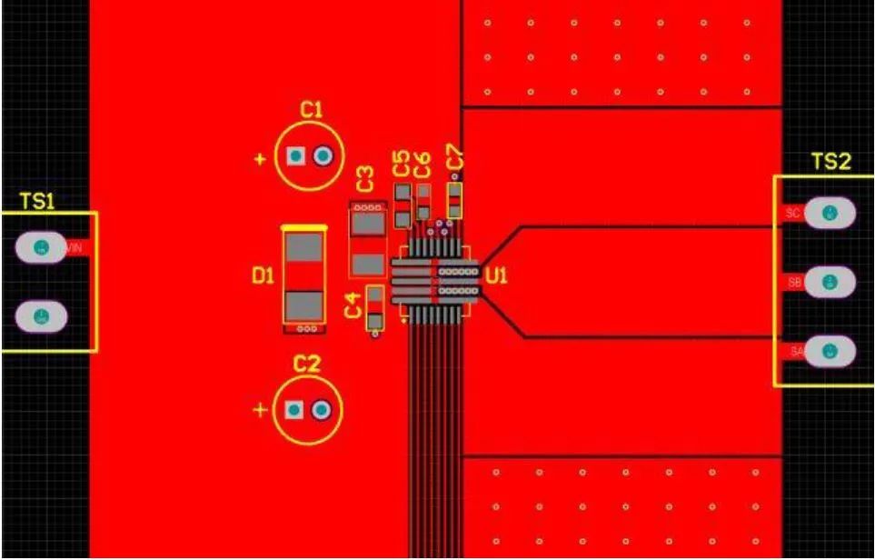
Figure 15: FCQFN PCB LayoutFigure 15 shows a power stage IC MP6540 from MPS Company. This device has long power and ground pads, along with three output pads. Note that this package is only 5mmx5mm.The copper area on the left side of the device is the power input pad. This larger copper area is directly connected to the device’s two power pads.The three output pads connect to the copper area on the right side of the device. Note how the copper area extends as much as possible after exiting the pad. This allows heat to be effectively transferred from the pad to the ambient air.Also, note the multiple rows of small vias in the two pads on the right side of the device. These pads are all grounded, and a solid ground layer is placed on the back of the PCB. The diameter of these vias is 0.46 mm, with a drilling diameter of 0.25 mm. The vias are small enough to fit within the pad area.In summary, to successfully implement PCB design using motor driver ICs, careful layout of the PCB is essential. Therefore, this article provides some practical suggestions to help PCB designers achieve good electrical and thermal performance for PCBs.Author: Pete Millett, Technical Marketing Engineer, Monolithic Power Systems, Translated by: Toffee Jia


 Click to read the original text and apply for free.