

Abstract: The layout of switch power supply PCBs is an important process in the development of power products. In many cases, a power supply that is perfectly designed on paper may not work properly during initial debugging due to various issues in the PCB layout. This article discusses the basic points of switch power supply PCB layout in detail and describes some practical PCB layout examples.
0 Introduction
In order to adapt to the rapid iteration of electronic products, product design engineers tend to choose AC/DC adapters that are easily available in the market and directly install multiple DC power supplies on the system’s circuit board. Since the electromagnetic interference generated by switch power supplies can affect the normal operation of electronic products, correct power supply PCB layout becomes very important. The layout of switch power supply PCBs is completely different from that of digital circuit PCBs. In digital circuit layouts, many digital chips can be automatically arranged by PCB software, and the connections between chips can also be automatically connected by PCB software. A switch power supply laid out using automatic layout methods will definitely not work properly. Therefore, designers need to have a certain understanding of the basic rules of switch power supply PCB layout and the working principles of switch power supplies.
1 Basic Points of Switch Power Supply PCB Layout
1.1 Capacitor High-Frequency Filtering Characteristics
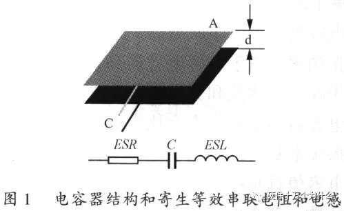
Figure 1 shows the basic structure of a capacitor and its high-frequency equivalent model.
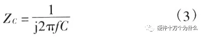
The basic formula for a capacitor is
Formula (1) shows that reducing the distance (d) between the capacitor plates and increasing the plate area (A) will increase the capacitance of the capacitor.
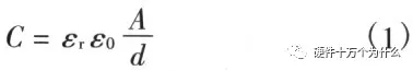
Capacitors typically have two parasitic parameters: equivalent series resistance (ESR) and equivalent series inductance (ESL). Figure 2 shows the impedance (Zc) of a capacitor at different operating frequencies.
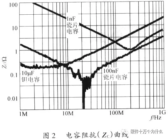
The resonant frequency (fo) of a capacitor can be derived from its capacitance (C) and equivalent series inductance (LESL), as follows:
When a capacitor operates at a frequency below fo, its impedance decreases as frequency increases, i.e.,
When a capacitor operates at a frequency above fo, its impedance increases as frequency increases, i.e.,

When the operating frequency of a capacitor approaches fo, the capacitive impedance equals its equivalent series resistance (RESR).
Electrolytic capacitors generally have large capacitance and high equivalent series inductance. Due to their low resonant frequency, they can only be used for low-frequency filtering. Tantalum capacitors typically have larger capacitance and lower equivalent series inductance, allowing them to be used for medium to high-frequency filtering. Ceramic capacitors usually have small capacitance and equivalent series inductance, resulting in a much higher resonant frequency than electrolytic and tantalum capacitors, making them suitable for high-frequency filtering and bypass circuits. Since the resonant frequency of small capacitance ceramic capacitors is higher than that of large capacitance ceramic capacitors, care should be taken not to select ceramic capacitors with excessively high capacitance values for bypass applications. To improve the high-frequency characteristics of capacitors, multiple capacitors with different characteristics can be connected in parallel. Figure 3 shows the effect of improved impedance when multiple capacitors with different characteristics are connected in parallel.
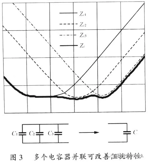
Basic point 1 of power supply layout: The capacitance of bypass ceramic capacitors should not be too large, and their parasitic series inductance should be minimized. Connecting multiple capacitors in parallel can improve the high-frequency impedance characteristics of the capacitors.
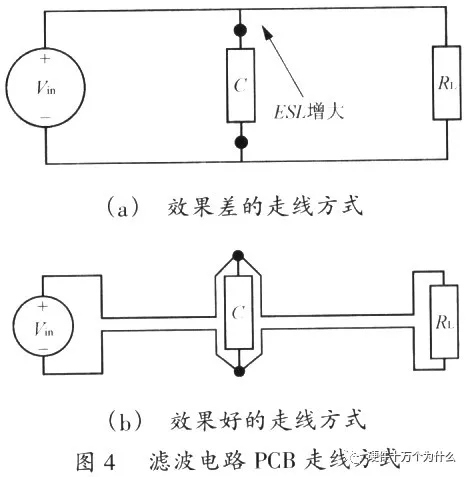
Figure 4 shows different routing methods for input power (Vin) to the load (RL) on a PCB. To reduce the ESL of the filter capacitor (C), the lead length should be minimized; the routing from the positive terminal of Vin to RL and from the negative terminal of Vin to RL should be kept as close as possible.
1.2 Inductor High-Frequency Filtering Characteristics
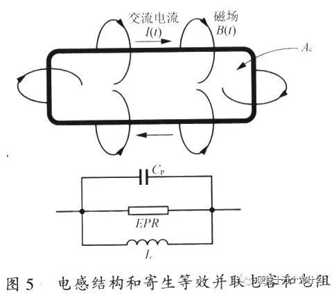
The current loop in Figure 5 is similar to the inductance of a one-turn coil. The electromagnetic field R(t) generated by high-frequency AC current will surround the inside and outside of this loop. If the area of the high-frequency current loop (Ac) is large, significant electromagnetic interference will be generated both inside and outside the loop.
The basic formula for inductance is
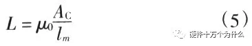
From formula (5), it can be seen that reducing the area of the loop (Ac) and increasing the loop perimeter (lm) can reduce L.
Inductors typically have two parasitic parameters: equivalent parallel resistance (EPR) and equivalent parallel capacitance (Cp). Figure 6 shows the impedance (ZL) of an inductor at different operating frequencies.
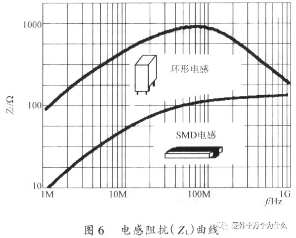
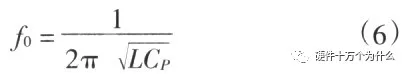
The resonant frequency (fo) can be derived from the inductance value (L) and its equivalent parallel capacitance (Cp), as follows:
When an inductor operates at a frequency below fo, its impedance increases as frequency increases, i.e.,

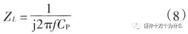
When an inductor operates at a frequency above fo, its impedance decreases as frequency increases, i.e.,
When the operating frequency of an inductor approaches fo, the inductive impedance equals its equivalent parallel resistance (REPR).
In switch power supplies, the Cp of inductors should be kept as small as possible. It should also be noted that inductors of the same inductance value can have different Cp values due to different coil structures. Figure 7 shows the different Cp values of inductors with the same inductance value under two different coil structures. Figure 7(a) shows that the 5-turn winding of the inductor is wound sequentially. The Cp value of this coil structure is 1/5 of the equivalent parallel capacitance (C) of a 1-turn coil. Figure 7(b) shows that the 5-turn winding of the inductor is wound in a crossed manner, where windings 4 and 5 are placed between windings 1, 2, and 3, and windings 1 and 5 are very close together. The Cp produced by this coil structure is twice that of a 1-turn coil.
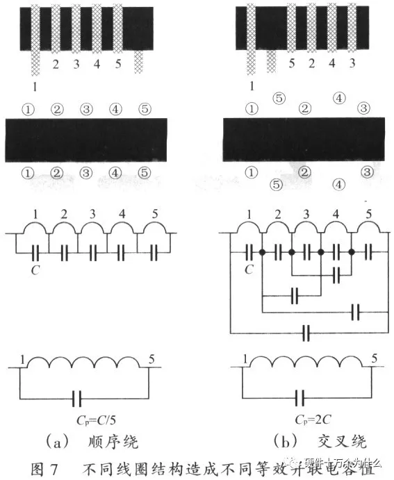
It can be seen that the Cp values of two inductors with the same inductance value can differ by several times. If the Cp value of an inductor is too large in high-frequency filtering, high-frequency noise can easily couple directly to the load through Cp. Such an inductor will lose its high-frequency filtering function.
Figure 8 shows different routing methods for Vin through L to the load (RL) on a PCB. To reduce the Cp of the inductor, the two pins of the inductor should be kept as far apart as possible. The routing from the positive terminal of Vin to RL and from the negative terminal of Vin to RL should be kept as close as possible.
1.3 Mirror Plane
The concept of the mirror plane in electromagnetic theory can greatly assist designers in mastering the PCB layout of switch power supplies. Figure 9 illustrates the basic concept of the mirror plane.
Figure 9(a) shows the scenario when DC current flows over a ground plane. At this time, the return DC current on the ground plane is very evenly distributed across the entire ground plane. Figure 9(b) shows the scenario when high-frequency current flows over the same ground plane. In this case, the return AC current can only flow in the middle of the ground plane, while there is no current at the edges of the ground plane. Once the concept of the mirror plane is understood, it becomes easy to see the routing issues on the ground plane in Figure 10. Designers should avoid placing any power or signal traces on the ground plane. Once traces on the ground plane disrupt the entire high-frequency loop, the circuit will generate strong electromagnetic radiation that disrupts the normal operation of surrounding electronic devices.
Basic point 3 of power supply layout: Avoid placing any power or signal traces on the ground plane.
1.4 High-Frequency Loop
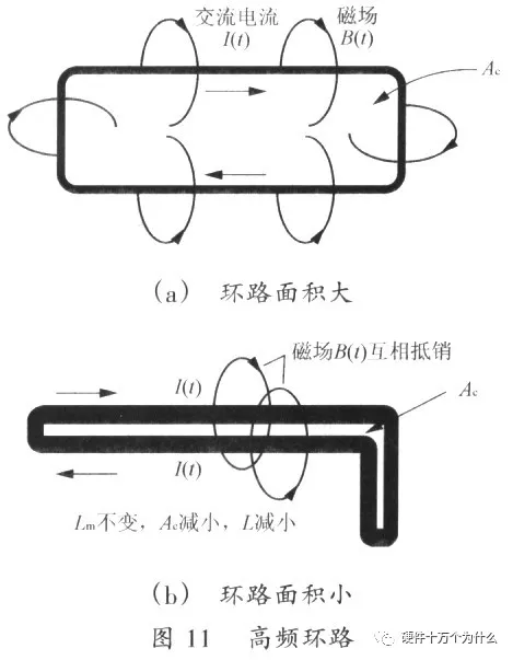
There are many high-frequency loops composed of power devices in switch power supplies. If the layout of these loops is not done well, it can greatly affect the normal operation of the power supply. To reduce the electromagnetic noise generated by high-frequency loops, the area of these loops should be kept very small. As shown in Figure 11(a), if the area of the high-frequency current loop is large, strong electromagnetic interference will be generated both inside and outside the loop. Conversely, if the area of the loop is designed to be very small, as shown in Figure 11(b), the electromagnetic fields inside and outside the loop will cancel each other out, making the entire circuit very quiet.
Basic point 4 of power supply layout: The area of high-frequency loops should be minimized.
1.5 Via and Pad Placement
Many designers like to place many vias on multilayer PCBs. However, it is essential to avoid placing too many vias on the return path of high-frequency currents. Otherwise, the routing of high-frequency currents on the ground plane will be disrupted. If it is necessary to place some vias on the high-frequency current path, space should be left between the vias to allow high-frequency currents to pass smoothly. Figure 12 shows the placement of vias.
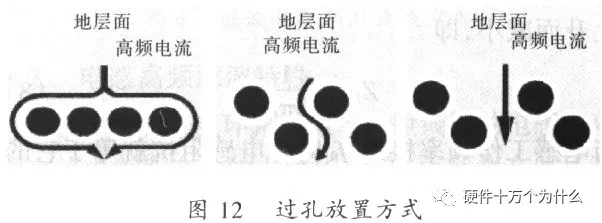
Basic point 5 of power supply layout: The placement of vias should not disrupt the flow of high-frequency currents on the ground plane.
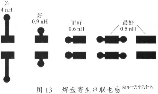
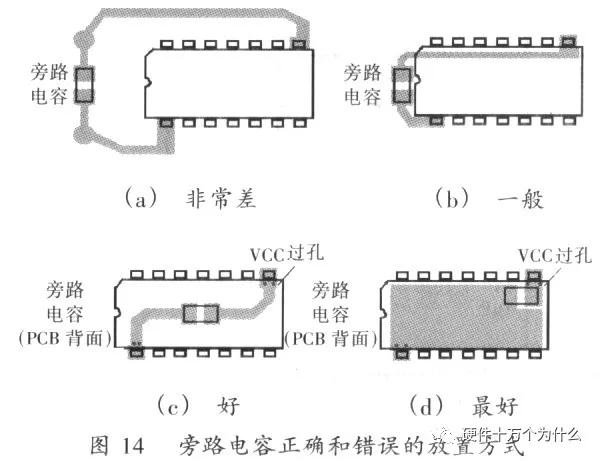
Designers should also note that different pad shapes will produce different series inductances. Figure 13 shows the series inductance values of several pad shapes.
The placement of bypass capacitors (Decouple) should also consider their series inductance values. Bypass capacitors must be low impedance and low ESL ceramic capacitors. However, if a high-quality ceramic capacitor is not placed correctly on the PCB, its high-frequency filtering function will be lost. Figure 14 shows the correct and incorrect placement of bypass capacitors.
1.6 Power Supply DC Output
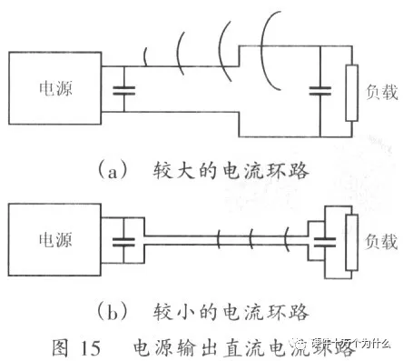
Many switch power supplies have loads that are far from the output port of the power supply. To avoid the output traces being affected by electromagnetic interference generated by the power supply itself or surrounding electronic devices, the output power traces must be kept very close, as shown in Figure 15(b), to minimize the area of the output current loop.
1.7 Ground Plane Separation on System Board
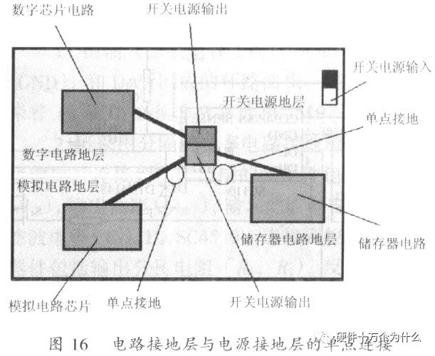
The next generation of electronic product system boards will simultaneously have analog circuits, digital circuits, and switch power supply circuits. To reduce the impact of power supply noise on sensitive analog and digital circuits, it is usually necessary to separate the ground planes of different circuits. If multilayer PCBs are used, the ground planes of different circuits can be separated by different PCB layers. If the entire product has only one layer of ground plane, separation must be done within that single layer as shown in Figure 16. Whether separating ground planes on multilayer PCBs or single-layer PCBs, the ground planes of different circuits should be connected to the ground plane of the switch power supply at a single point.
Basic point 6 of power supply layout: Different circuits on the system board require different ground planes, and the ground planes of different circuits should be connected to the power supply ground plane at a single point.
2 Examples of Switch Power Supply PCB Layout
The schematic diagram of a switch power supply. Designers should be able to distinguish between components in the power circuit and those in the control signal circuit on this schematic. If designers treat all components in this power supply as components in a digital circuit, the problems will be quite serious. Generally, it is first necessary to know the path of high-frequency current in the power supply and distinguish between small signal control circuit components and power circuit components and their traces. In general, the power circuit of the power supply mainly includes input filter capacitors, output filter capacitors, filter inductors, and power MOSFETs at both ends. The control circuit mainly includes PWM control chips, bypass capacitors, bootstrap circuits, feedback voltage divider resistors, and feedback compensation circuits.
2.1 Power Circuit PCB Layout
The correct placement and routing of power devices on the PCB will determine whether the entire power supply operates normally. Designers must first have a certain understanding of the voltage and current waveforms on the power devices of the switch power supply.
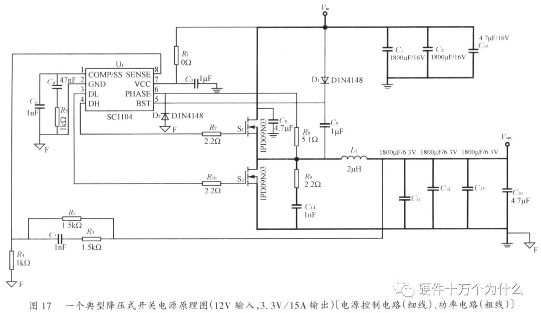
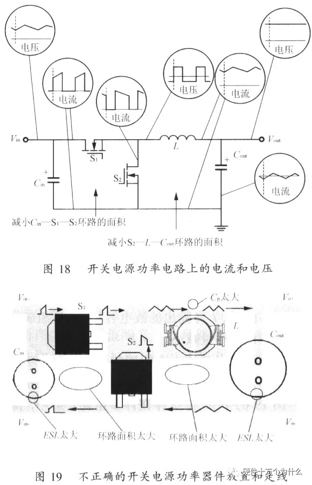
Figure 18 shows the current and voltage waveforms of the components in a buck switch power supply circuit. Since the current flowing through the input filter capacitor (Cin), upper MOSFET (S1), and lower MOSFET (S2) is AC current with high frequency and peak values, the area of the loop formed by Cin-S1-S2 should be minimized. Similarly, the area of the loop formed by S2, L, and output filter capacitor (Cout) should also be minimized.
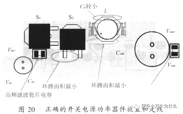
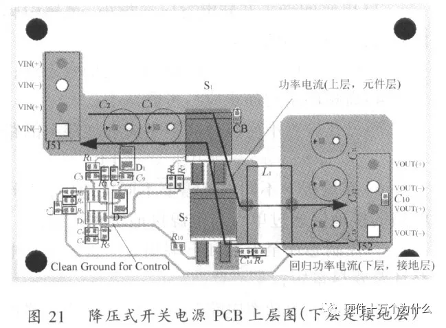
If designers do not follow the points mentioned in this article to create the power circuit PCB, they may end up with a power PCB as shown in Figure 19, which has many errors in layout: First, due to the large ESL of Cin, the high-frequency filtering capability of Cin is almost lost; second, the area of the Cin-S1-S2 and S1-L-Cout loops is too large, and the electromagnetic noise generated will greatly disturb the power supply itself and surrounding circuits; third, the pads of L are too close, resulting in a large Cp that reduces its high-frequency filtering function; fourth, the lead length of Cout is too long, resulting in a large ESL that loses high-frequency filtering capability. The areas of the Cin-S1-S2 and S2-L-Cout loops have been minimized. The connection point between the source of S1, the drain of S2, and L is a solid copper pad. Since the voltage at this connection point is high frequency, S1, S2, and L need to be very close together. Although there are no high peak high-frequency currents in the routing between L and Cout, a wider trace can reduce DC resistance losses and improve the efficiency of the power supply. If cost allows, the power supply can use a double-sided PCB with one side completely as a ground plane, but care must be taken to avoid routing power and signal lines on the ground plane. Additionally, a ceramic capacitor is added at both the input and output ports of the power supply to improve high-frequency filtering performance.
2.2 Control Circuit PCB Layout
The PCB layout of the power control circuit is also very important. An unreasonable layout can cause drift and oscillation of the output voltage of the power supply. The control lines should be placed next to the power circuit and must not be placed in the middle of high-frequency AC loops. Bypass capacitors should be as close as possible to the Vcc and ground pins (GND) of the chip. Feedback voltage divider resistors should also be placed near the chip. The loop from the chip driving the MOSFETs should also be kept as short as possible.
Basic point 7 of power supply layout: The driving circuit loop from the control chip to the upper and lower MOSFETs should be kept as short as possible.
2.3 Example 1 of Switch Power Supply PCB Layout
Figure 21 shows the component side routing diagram of the PCB in Figure 17. This power supply uses a low-cost PWM controller (Semtech model SC1104A). The bottom layer of the PCB is a complete ground plane. There is no separation between the power ground plane and the control ground plane in this PCB. It can be seen that the power circuit of this power supply runs from the input socket (top left of the PCB) through input filter capacitors (C1, C2), S1, S2, L1, output filter capacitors (C10, C11, C12, C13), to the output socket (bottom right of the PCB). SC1104A is placed at the bottom left of the PCB. Since the power circuit current does not pass through the control circuit on the ground plane, there is no need to separate the control circuit ground plane from the power circuit ground plane. If the input socket is placed at the bottom left of the PCB, then the power circuit current would directly pass through the control circuit, and it would then be necessary to separate the two.
2.4 Example 2 of Switch Power Supply PCB Layout
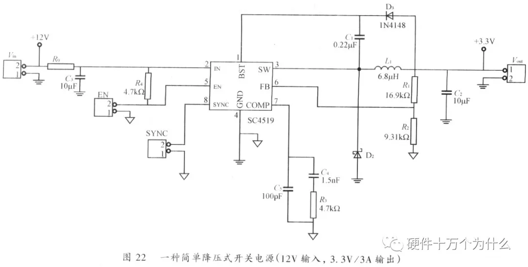
Figure 22 shows another buck switch power supply that converts a 12V input voltage to a 3.3V output voltage, with an output current of up to 3A. This power supply uses an integrated power controller (Semtech model SC4519). This controller integrates a power MOSFET within the power controller chip. Such a power supply is very simple and particularly suitable for applications in portable DVD players, ADSL, set-top boxes, and other consumer electronics.
Similar to the previous example, the following points should also be noted in the PCB layout of this simple switch power supply.
1) The area of the loop formed by the input filter capacitor (C3), the ground pin (GND) of SC4519, and D2 must be small. This means that C3 and D2 must be very close to SC4519.
2) A separated power circuit ground plane and control circuit ground plane can be used. Components connected to the power ground plane include the input socket (VIN), output socket (VOUT), input filter capacitor (C3), output filter capacitor (C2), D2, and SC4519. Components connected to the control ground plane include output voltage divider resistors (R1, R2), feedback compensation circuits (R3, C4, C3), enable socket (EN), and sync socket (SYNC).
3) A via should be added near the ground pin of SC4519 to connect the power circuit ground plane and the control signal ground plane at a single point.
Figure 23 shows the routing diagram of the upper layer of this power supply PCB. To facilitate reader understanding, the power ground plane and control signal ground plane are represented in different colors. Here, the input socket is placed at the top of the PCB, while the output socket is placed at the bottom of the PCB. The filter inductor (L1) is placed on the left side of the PCB and close to the power ground plane, while the feedback compensation circuit (R3, C4, C5), which is more sensitive to noise, is placed on the right side of the PCB and close to the control signal ground plane. D2 is very close to pins 3 and 4 of SC4519. Figure 24 shows the routing diagram of the lower layer of this power supply PCB. The input filter capacitor (C3) is placed on the lower layer of the PCB and very close to SC4519 and the power ground plane.
2.5 Example 3 of Switch Power Supply PCB Layout
Finally, we discuss the PCB layout points for a multi-output switch power supply. This power supply has three input voltages (12V, 5V, and 3.3V) and four output voltages (3.3V, 2.6V, 1.8V, and 1.2V). This power supply uses an integrated multi-channel switch controller (Serotech model SC2453). SC2453 provides a wide input voltage range of 4.5V to 30V, two switching frequencies of up to 700kHz, and output currents of up to 15A, as well as a low output voltage of 0.5V for synchronous buck converters. It also provides a dedicated adjustable positive linear regulator and a dedicated adjustable negative linear regulator. The TSSOP-28 package reduces the required PCB area. The two asynchronous buck converters can reduce input current ripple. Figure 25 is the schematic diagram of this multi-output switch power supply. The 3.3V output is generated from the 5V input, the 1.2V output is generated from the 12V input, and the 2.6V and 1.8V outputs are generated from the 3.3V input. Since all components on this power supply must be placed on a relatively small PCB area, the power ground plane and control signal ground plane must be separated. Referring to the points discussed in previous sections, first distinguish between components connected to the power ground plane and those connected to the control signal ground plane, then place the control signal components on the signal ground plane close to the SC2453, and connect the power ground plane and control signal ground plane at a single point. This connection point is usually chosen at the ground pin of the control chip (pin 21 in SC2453). Figure 26 details the layout of this power supply.
Basic point 8 of power supply layout: Components in the power circuit and control signal circuit of the switch power supply need to connect to different ground planes, and these two ground planes are generally connected at a single point.
3 Conclusion
The eight key points of switch power supply PCB layout are:
1) The capacitance of bypass ceramic capacitors should not be too large, and their parasitic series inductance should be minimized. Connecting multiple capacitors in parallel can improve the impedance characteristics of the capacitors;
2) The parasitic parallel capacitance of inductors should be minimized, and the distance between inductor pin pads should be as far apart as possible;
3) Avoid placing any power or signal traces on the ground plane;
4) The area of high-frequency loops should be minimized;
5) The placement of vias should not disrupt the flow of high-frequency currents on the ground plane;
6) Different circuits on the system board require different ground planes, and the ground planes of different circuits should be connected to the power ground plane at a single point;
7) The driving circuit loop from the control chip to the upper and lower MOSFETs should be kept as short as possible;
8) Components in the power circuit and control signal circuit of the switch power supply need to connect to different ground planes, and these two ground planes are generally connected at a single point.

Some screenshots of electronic books
Complete set of hardware materials collection