Source: Chip Intelligence

1. Definition and Classification of FPGA Chips
1. Definition and Physical Structure of FPGA Chips
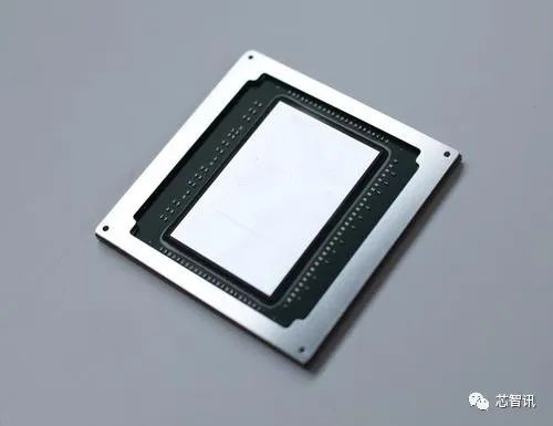
FPGA (Field Programmable Gate Array) chips are developed based on programmable devices (PAL, GAL) and are semi-custom, programmable integrated circuits.
Inventor: Ross Freeman, co-founder of Xilinx, invented the FPGA integrated circuit structure in 1984. The world’s first commercial FPGA chip was the Xilinx XC4000 series FPGA product.
FPGA chips process signals in a fixed pattern and can perform new types of tasks (computational tasks, communication tasks, etc.). Compared to Application-Specific Integrated Circuits (ASICs), FPGA chips are more flexible and can add a larger number of circuit components than traditional programmable devices to achieve diverse functions.
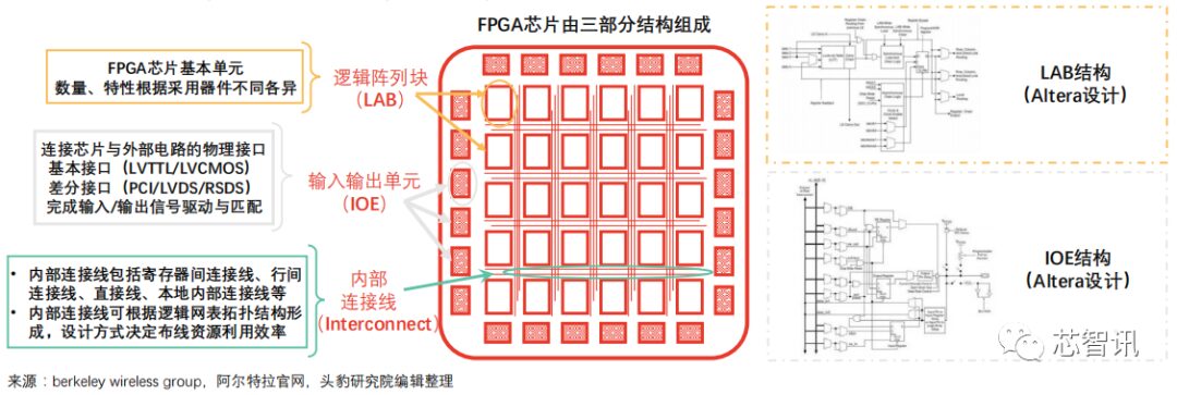
Physical Structure: FPGA chips mainly consist of three parts: IOE (Input Output Element), LAB (Logic Array Block, defined by Xilinx as Configurable Logic Block CLB), and Interconnect (internal connections).
2. Characteristics and Classification of FPGA Chips
FPGA chips have significant advantages in real-time performance (fast data signal processing speed) and flexibility, occupying an irreplaceable position in the field of deep learning, while also being characterized by high development difficulty.
FPGA chips have the following characteristics:
Strong Applicability: They are one of the devices with the shortest development cycle and lowest application risk among dedicated circuits (some customers can obtain applicable FPGA chips without investing in R&D).
Parallel Computing: The internal structure of FPGA can build corresponding numbers of pipelines based on the number of data packets, with different pipelines processing different data packets, achieving pipeline parallelism and data parallelism.
Strong Compatibility: FPGA chips can be compatible with large-scale integrated circuits such as CMOS and TTL, working together to complete computational tasks.
Flexible Design: They belong to hardware-reconfigurable chip structures, with a rich number of input-output unit pins and triggers set internally.
Enhanced Status: Initially, they were batch substitutes for ASIC chips in some application scenarios; recently, with the expansion of data center scales by leading internet companies such as Microsoft, the application range of FPGA chips has expanded.
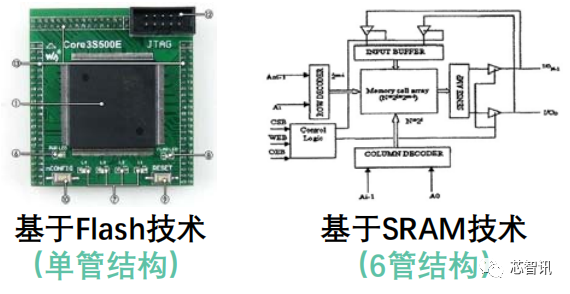
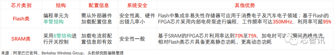
FPGA manufacturers mainly provide FPGA chips based on two types of technologies: Flash technology and SRAM technology (Static Random-access Memory). Both types of technology can achieve system-level programming functions and have high computing performance, with system gate array density exceeding 1 million.
Core Differences: Flash-based programmable devices have non-volatile characteristics, meaning that stored data does not disappear when the current is turned off. In contrast, SRAM-based FPGA chips do not have non-volatile characteristics and are the most widely used architecture.
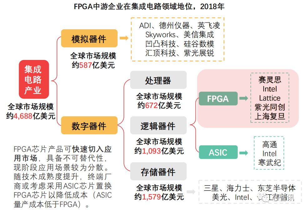
2. Comparison of FPGA Chips with Other Mainstream Chips
The CPU is a general-purpose device, while the FPGA architecture emphasizes computational efficiency compared to the CPU architecture. Relying on FPGA’s parallel computing to process visual algorithms can significantly enhance computational speed and reduce latency.
1. FPGA Chips Compared to CPU Chips
CPU Processing of Computational Instruction Flow: The CPU receives task instructions through a dedicated decoder, with the reception process divided into two steps: instruction fetching (the CPU extracts execution instructions from a dedicated instruction storage) and instruction translation (translating instructions into data according to specific rules and transmitting them to the computing unit). The computing unit consists of transistors (the basic elements of the CPU), where “on” and “off” correspond to “1” and “0” machine code digits. CPU processing characteristics include: • The physical structure of the CPU includes Control (instruction fetching, instruction translation), Cache (temporary instruction storage), and ALU (Arithmetic Logic Unit, occupying about 20% of CPU space).
The CPU is a core for processing general computing tasks, capable of handling computing requests from multiple devices and can terminate current calculations at any time to switch to other calculations. • The logic control unit and instruction translation structure are relatively complex, allowing for resuming calculations from interrupt points, sacrificing computational efficiency for achieving high generality.
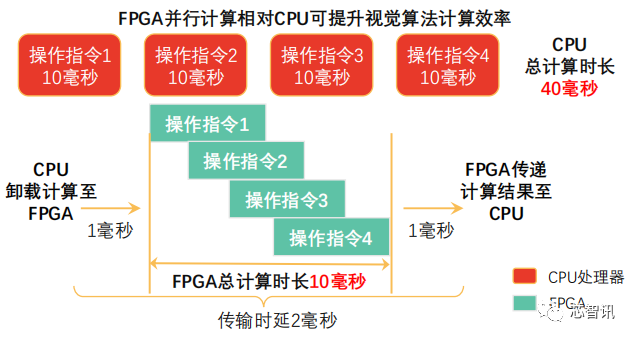
Comparison of CPU Visual Algorithms and FPGA Visual Algorithms:
CPU Architecture: When the CPU processes visual algorithms, it must execute instructions in a specified order, with the first instruction starting after the overall image processing is complete, and the second instruction begins. In a 4-step operation instruction environment, setting a single operational instruction requires 10 milliseconds, with a total algorithm completion time of about 40 milliseconds.
FPGA Architecture: The FPGA processes visual algorithms using a large-scale parallel computing model, allowing 4-step operational instructions to run simultaneously within different pixels of an image. Setting a single operational instruction requires 10 milliseconds, with the FPGA completing the overall visual algorithm processing time of the image in just 10 milliseconds, significantly faster than the CPU.
“FPGA + CPU” Architecture: In this architecture, images are transmitted between the CPU and FPGA, with the overall processing time of the algorithm including transmission time still lower than that of a pure CPU architecture.
Algorithm Example: Taking the convolution filter image sharpening computational task as an example, the system must run the image through a threshold to produce a binary image. Under the CPU architecture, the system must complete the overall convolution step before the threshold step, while the FPGA supports the same algorithm running simultaneously, resulting in a convolution calculation speed improvement of approximately 20 times compared to the CPU architecture.
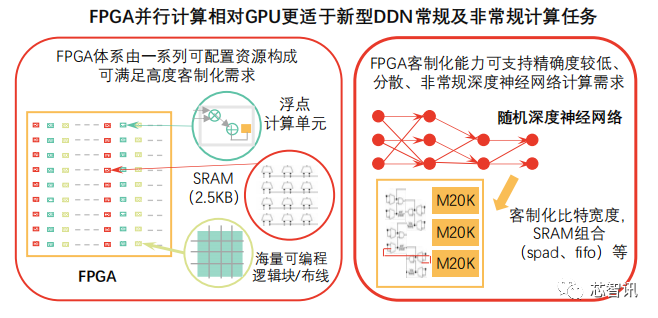
2. FPGA Chips Compared to GPU Chips
GPU Physical Structure: The GPU is a graphics processor, performing calculations for various computer graphics rendering behaviors (such as vertex setting, light and shadow operations, pixel operations, etc.). A standard GPU includes a 2D engine, a 3D engine, a video processing engine, and a video memory management unit. Among them, the 3D engine contains T&L units, Pixel Shader, etc.
GPU Processing of Computational Instruction Flow:
Vertex Processing: The GPU reads 3D graphic vertex data, determining the shape and positional relationships of 3D graphics based on appearance data, establishing the skeleton of the 3D graphics.
Rasterization Calculation: Display images consist of pixels, and the system must convert graphic points and lines into pixel points through algorithms. Converting vector graphics into pixel points is the rasterization calculation process.
Texture Mapping: Texture mapping is performed on the multi-deformable surfaces to generate realistic graphics.
Pixel Processing: The GPU computes and processes the pixels completed by rasterization, determining the final attributes of the pixels, mostly accomplished through Pixel Shader.
Comparison of GPU and FPGA Characteristics:
Peak Performance: The GPU’s peak computing performance (10 Tflops) is significantly higher than the FPGA’s peak performance (less than 1 Tflops). The GPU architecture relies on deep pipelining and other technologies to achieve manual circuit customization based on standard cell libraries. In contrast, FPGA design resources are limited, and model selection determines the logical resource upper limit (floating-point operation resources occupy a high percentage), with FPGA logic units based on SRAM lookup tables and limited wiring resources.
Memory Interface: The GPU memory interface (double data rate memory, etc.) has better bandwidth than the DDR (double data rate synchronous dynamic random-access memory) interface used by FPGA, meeting the frequent memory access needs of machine learning.
Flexibility: FPGA can program hardware based on specific applications, while GPU design cannot change hardware resources after completion. In the long term, machine learning uses multiple instructions to process a single data point, and FPGA hardware resource flexibility can better meet the needs.
Power Consumption: The average power consumption of GPU (200W) is significantly higher than that of FPGA (10W), effectively solving the heat dissipation problem.
3. FPGA Chips Compared to ASIC Chips
ASIC chips have a high degree of specialization, and the non-repetitive costs (tape-out) of the development process are extremely high. In the early stages of 5G commercialization, FPGAs can seize the market with their flexibility, but in large-scale mass production scenarios, ASIC chips have a competitive advantage.
Differences in Development Processes Between ASIC and FPGA:
ASIC needs to be designed from standard cells, and when functional and performance requirements change, the ASIC chip design must undergo re-tape-out, leading to high time and economic costs in the design process.
FPGA includes prefabricated gates and triggers, with programmable interconnection characteristics that allow for chip function reconfiguration. In contrast, ASIC chips rarely possess reconfiguration capabilities.
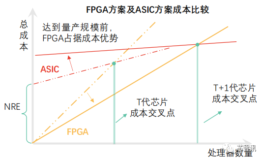
Differences in Economic and Time Costs Between ASIC and FPGA: The ASIC design process involves fixed costs, resulting in less material waste during the design process, while the relative repetitive costs of FPGA are lower, but the non-repetitive costs are higher (averaging over one million dollars).
FPGA’s repetitive costs are higher than those of comparable ASIC chips, and in large-scale mass production scenarios, the unit IC cost of ASIC chips continues to decrease with increasing output, significantly lowering total costs compared to FPGA chips.
FPGA can be used immediately after programming without waiting for chip tape-out cycles, which helps companies save product launch time compared to ASIC.
During the immature stage of technology, FPGA architecture supports flexible changes in chip functionality, helping to reduce device product costs and risks, making it more suitable for the market environment in the early stages of 5G commercialization.
3. Analysis of China’s FPGA Chip Industry Chain
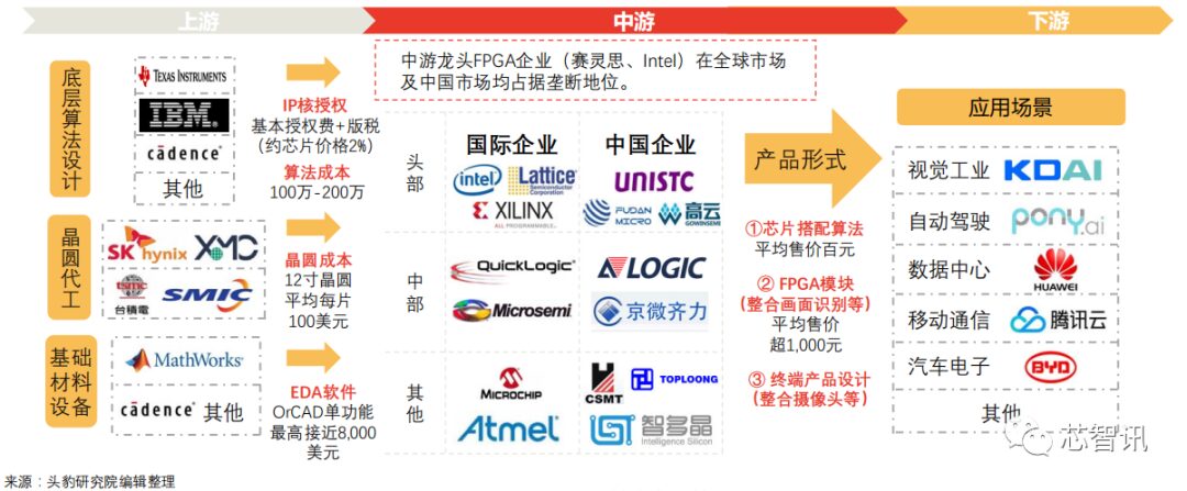
FPGA chips constitute an important submarket of artificial intelligence chips, with a lengthy industry chain. FPGA manufacturers, as midstream companies, have strong bargaining power with upstream software, hardware suppliers, and downstream customer enterprises.
The FPGA chip industry chain in China consists of upstream algorithm design companies, EDA tool suppliers, wafer foundries, specialized materials and equipment suppliers, midstream various FPGA chip manufacturers, packaging and testing manufacturers, and downstream application scenario customer enterprises including visual industry manufacturers, automotive manufacturers, communication service providers, and cloud data centers.
1. Analysis of China’s FPGA Chip Industry Chain Upstream
As a programmable device, FPGA chips have fewer tape-out requirements and a lower dependency on upstream foundries, requiring specialized design software and algorithm architecture support.
Bottom-layer algorithm architecture design companies have a low dependency on bottom-layer algorithm architecture for FPGA chip design, and the bargaining power of upstream algorithm suppliers over midstream FPGA chip R&D and manufacturing companies is limited. Foreign algorithm architecture design companies include Qualcomm, ARM, Google, Microsoft, IBM, etc.
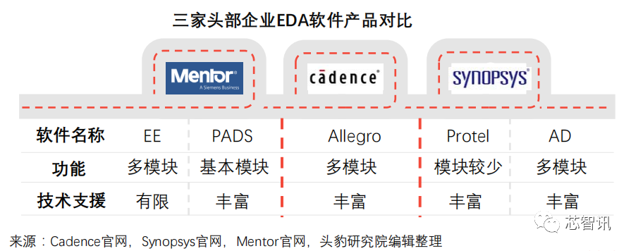
Specialized software suppliers: FPGA chip companies need to complete designs using development auxiliary software such as EDA (Quartus, Vivado, etc.). International top-tier companies (such as Synopsys) that can provide EDA software charge high module usage fees to chip R&D companies. There are relatively few companies in the Chinese market that can provide EDA products, represented by companies such as Chipone, BGI, and Boda Microelectronics. Chinese EDA companies started R&D relatively late, and the stability and maturity of software products need to be improved. Chinese FPGA R&D companies face high costs when purchasing foreign EDA software products, and in the long term, domestic EDA companies need to eliminate the gap with foreign counterparts to provide price-friendly EDA products for midstream chip companies.
Currently, there are about 30 mainstream wafer fabs in China, covering specifications of 8-inch wafers and 12-inch wafers. Among them, there are relatively more 8-inch wafer fabs than 12-inch wafer fabs. Domestic 12-inch wafer fabs in China include Wuhan Xinxin, SMIC, and Unisoc, with an average monthly production capacity of about 65,000 wafers. Foreign manufacturers that have established wafer fabs in China include Intel, SK Hynix, etc. The development speed of Chinese wafer fabs is relatively fast, with Wuhan Xinxin’s 12-inch wafer fab exceeding SK Hynix’s average monthly production capacity of 160,000 wafers, reaching an average monthly production capacity of 200,000 wafers.
2. Analysis of China’s FPGA Chip Industry Chain Midstream
Midstream companies in China’s FPGA chip industry have a large profit margin. With the accumulation of R&D capabilities and the maturity of application markets, the midstream industry pattern may undergo a transformation, shifting from hardware and device R&D to software and platform development.
FPGA Chip Profit Margin is Huge:
Compared to CPU, GPU, ASIC, and other products, FPGA chips have a relatively high profit margin.
Mid-to-low density million-gate and ten-million-gate FPGA chip R&D companies have profit margins close to 50% (comparable to the iPhone’s gross margin of nearly 50%). High-density billion-gate FPGA chip R&D companies have profit margins nearing 70% (taking Xilinx and Intel’s acquisition of Altera as examples).
Chinese Midstream Companies Face Market Potential Release Node:
Compared to giants like Xilinx and Intel, China’s FPGA R&D started late, but the R&D progress is gradually catching up (the gap with global leading manufacturers has narrowed from 3 generations to about 2 generations).
Since 2017, China’s FPGA has entered a critical development stage (transitioning from reverse design to forward design). During this reporting period, under the backdrop of intensified China-U.S. trade friction, midstream companies in China’s FPGA industry that have completed initial accumulations face good development opportunities. Compared to the global integrated circuit market with a scale of over $460 billion, the FPGA market is relatively small and has room for incremental release.
Industry Pattern May Change:
As the concentration of midstream companies in the FPGA industry increases, the industry pattern may undergo a transformation. Chinese companies can adjust market strategies to shift from hardware R&D to software design and from device R&D to platform construction.
3. Analysis of China’s FPGA Chip Industry Chain Downstream
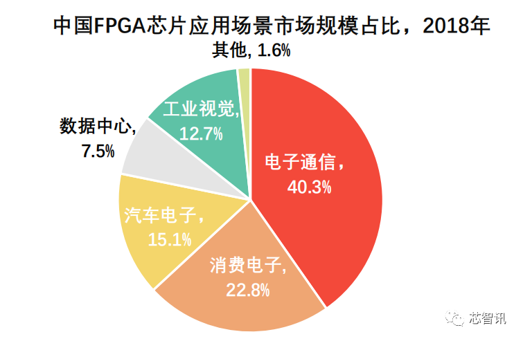
The downstream application market for China’s FPGA chip industry is extensive, with electronic communication and consumer electronics occupying the top positions, while industrial control, robotics, video control, autonomous driving, and servers have significant growth potential across multiple fields.
FPGA manufacturers focus on the communication market and consumer electronics scenarios. The Chinese FPGA application market is mainly in consumer electronics and communication. Domestic chips lag behind high-end foreign products in hardware performance, lacking competitiveness in the high-end civilian market, but short-term shipments are high in fields such as LED displays and industrial vision. With technological breakthroughs from Chinese companies and the maturity of 5G technology, Chinese FPGA manufacturers may achieve high growth in market share in the communication field.
Automotive and data center applications follow closely. After 2025, edge computing technology and cloud computing technology will be fully deployed in smart traffic networks and supercomputing centers, with the FPGA application market growth rate in autonomous driving and data centers expected to exceed that of communication and consumer electronics markets.
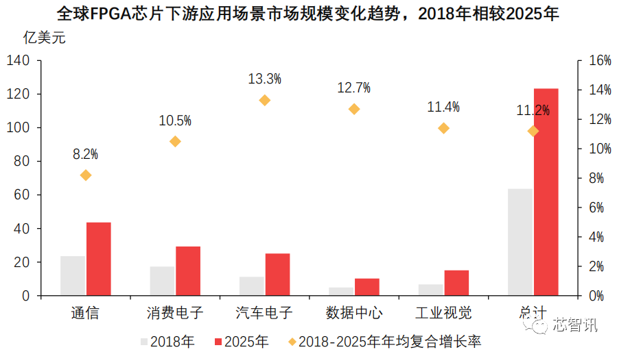 Growth of FPGA Chip Downstream Application Market Scale: In 2018, communication, consumer electronics, and automotive scenarios constituted over 80% of the total demand for global FPGA chips, and the market scale continues to expand. FPGA devices, as core components of 5G base stations, automotive terminal devices, and edge computing devices, have significant acceleration effects and face certain incremental demand in the downstream market. With the strengthening of midstream domestic enterprises, domestic FPGA chip products may enter the downstream market with a price advantage, reducing the procurement costs of downstream enterprises for high-end programmable devices.
4. Market Scale of China’s FPGA Chip Industry
The demand for FPGA chips continues to rise in application scenarios, with the development of 5G and artificial intelligence technologies promoting the expansion of China’s FPGA market and stimulating the release of incremental demand.
1. Market Scale of the FPGA Chip Industry
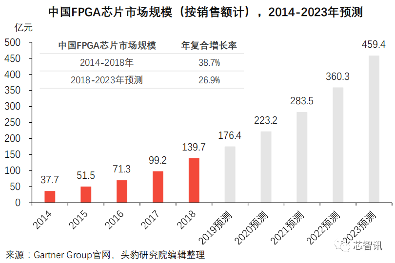
As the downstream application market expands, the market scale of China’s FPGA industry continues to rise. In 2018, the FPGA market scale in China approached 14 billion yuan. The development of new 5G communication technologies and machine learning technologies will further stimulate the expansion of China’s FPGA market. It is expected that by 2023, the market scale of China’s FPGA chip market will approach 46 billion yuan.
Global FPGA Market Scale Potential Will Be Released, Mainly Benefiting From the Following Factors:
Downstream application scenarios are becoming increasingly diverse: FPGA chips are more flexible than ASICs, saving tape-out time costs and shortening time to market. The application scenarios have expanded from communication transceivers and consumer electronics to automotive electronics, data centers, high-performance computing, industrial vision, and medical testing. In the short term, the Chinese FPGA application scenarios remain dispersed, with both stock and incremental markets having room for expansion.
Some application scenarios are irreplaceable: FPGA chips have advantages in low R&D costs and manufacturing costs in scenarios where technology is unstable, flexibility is highly demanded, and demand volumes are small (devices can be programmed on-site according to specific needs).
Global Market Share Analysis:
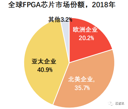
The Asia-Pacific market demand is significant. The Asia-Pacific region is the main application market for FPGAs, accounting for over 40% of the global market share. By the end of 2018, China’s FPGA market scale approached 14 billion yuan, facing significant incremental demand space with the expansion of 5G communication infrastructure.
North American giants dominate the top market. In North America, Xilinx and Intel (acquiring Altera) maintain a duopoly in the FPGA market. In the Chinese FPGA market, Xilinx holds over 50% market share, while Intel’s share is close to 30%.
5. The Complexity of FPGA Chip Design Continues to Increase
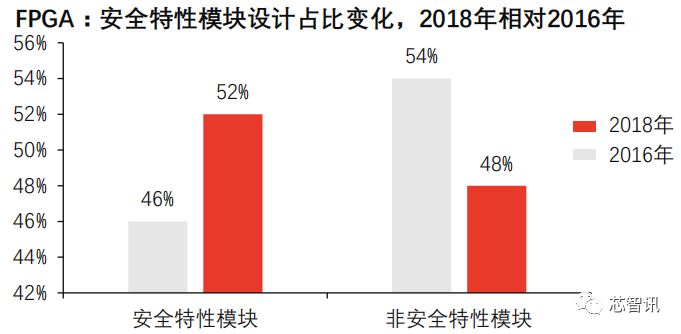
From 2016 to 2018, the proportion of high-performance, high-security programmable chip design projects in the global FPGA R&D field increased, leading to an increase in FPGA design complexity.
The demand for security features has increased, raising the complexity of high-performance FPGA chip designs.
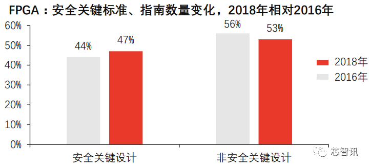
Increase in Security Critical Standards and Guidelines:
The increase in demand for security features can be expressed by the increase in security critical standards and guidelines. In 2016 and prior, most FPGA development projects were based on a single security critical standard, while from 2018 onwards, more FPGA R&D projects are developed based on one or more security critical standards and guidelines.
Increase in Security Assurance Hardware Module Design Projects:
Security assurance hardware module designs are widely used in areas such as encryption keys, digital rights management keys, passwords, and biometric reference data. Compared to 2016, the proportion of global FPGA security feature module design projects significantly increased in 2018 (with an increase of over 5%). The enhancement of security features increases the demand for design verification and verification complexity.
Other Design Projects Increase Chip Verification Complexity:
1. Increase in the Number of Embedded Processor Cores: Compared to 2016, more FPGA designs in 2018 tend towards SoC-class designs. In 2018, over 40% of FPGA designs included 2 or more embedded processors, and nearly 15% included 4 or more embedded processors, increasing the complexity of verification processes.
2. Increase in the Number of Asynchronous Clock Domains: In 2018, about 90% of FPGA design projects included 2 or more asynchronous clock domains, increasing the verification workload (verification models tend to be complex, and code exceptions increase).
6. Application Scenarios and Market Demand
1. Widely Used in Machine Learning Reinforcement Projects
FPGA chips are more suitable for non-fixed, non-standard machine learning evolutionary environments.
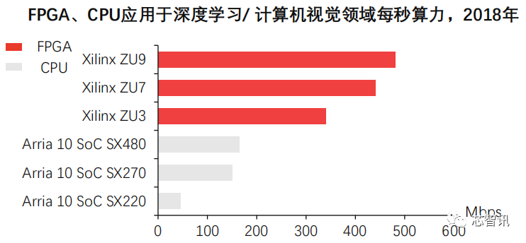
FPGA performs excellently in machine learning. Performance comparisons can refer to Xilinx’s public test results, which compare the performance of the reVISION series FPGA chips with NVIDIA’s Tegra X1 series GPU chips in the field of machine learning. Data shows that the FPGA solution outperforms the GPU solution by 6 times in terms of image capture speed per unit power consumption and by 42 times in frame rate for computer vision processing, while the FPGA’s latency is 1/5 that of the GPU. Comparing Xilinx FPGA with Intel’s Arria 10 SoC series CPU devices, Xilinx FPGA devices can enhance deep learning and computer vision computational efficiency by 3 to 7 times.
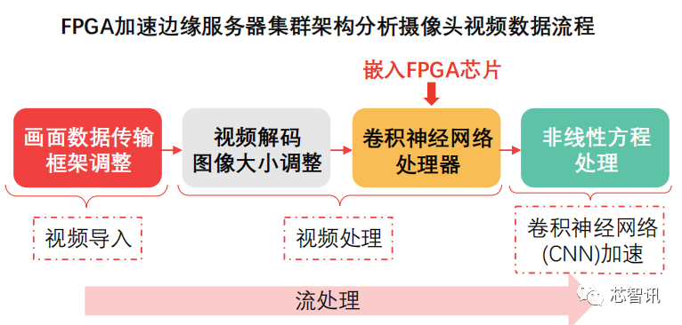
Companies Adopting New Architectures (Visual Data Transmission to FPGA Accelerates Edge Server Clusters):
FPGA optimizes stream processing. FPGA solutions can optimize stream processing for video analysis and deep learning inference (one of the big data processing techniques). Based on their flexible programming characteristics, FPGA solutions can meet reconfiguration needs, suitable for general models such as inventory management, fraud control, facial recognition, as well as complex models such as tracking, natural language interaction, and emotional detection.
Startups actively adopt FPGA solutions. Startups like Megh Computing and PointR.ai are actively adopting FPGA solutions to establish new video data processing architectures, leveraging compact, low-power computing module advantages.
△Source: Wilson Research Group and Mentor, edited by Leopard Research Institute
2. 5G Communication System Construction Increases Demand for FPGA Chips
The communication scenario is the most widely used application scenario for FPGA chips in the downstream of the industry chain (accounting for about 40%). With the development of 5G communication technology and hardware equipment upgrades (innovation in base station antenna transceivers), FPGA faces strong market demand drivers.
5G communication is about to be commercially scaled, driving an increase in FPGA chip usage and price release space.
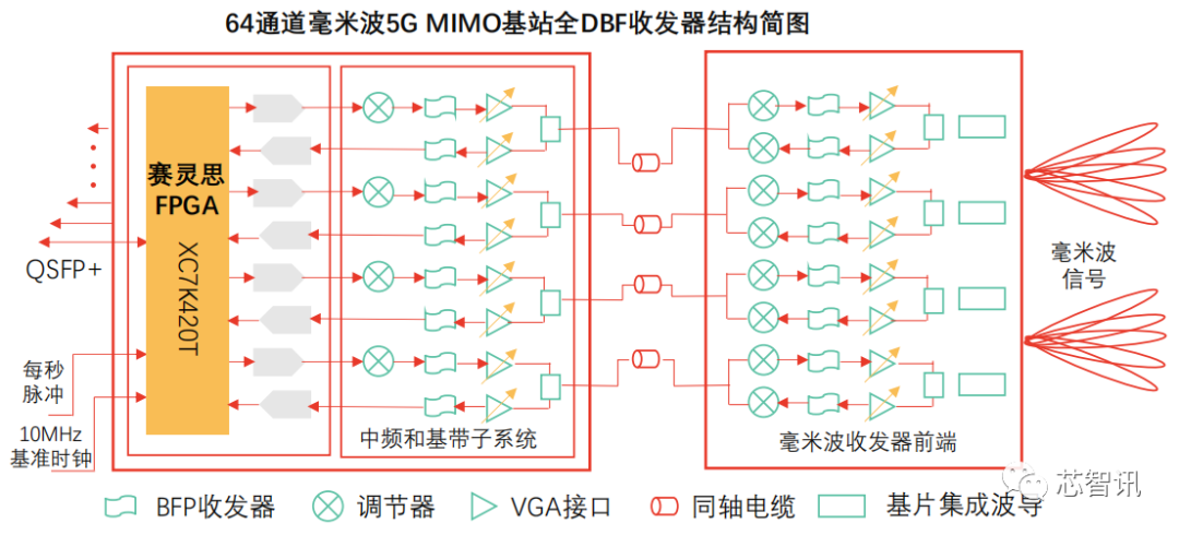
New Base Station Antenna Transceivers Use FPGA Chips. Under the Massive MIMO base station technology conditions of the 5G era, the number of base station transceiver channels has increased from 16T16R (dual-mode solution) to a maximum of 128T128R, and FPGA chips can be used to achieve multi-channel signal beamforming. For example, the mid-frequency and baseband subsystems of a 64-channel millimeter-wave MIMO full DBF transceiver use Xilinx Kintex-7 series FPGA. The mid-frequency and baseband subsystems together achieve general wireless access functionality.
Industry experts with over 10 years of product development and algorithm research experience in the FPGA chip industry indicate that FPGA has advantages over CPU and GPU in terms of power consumption and computational speed. Communication equipment companies will increase the application of FPGA devices in core equipment such as base station antenna transceivers (for example, leading mobile communication equipment manufacturers like Jingxin Communication embed FPGA chips in new transceiver products).
The global FPGA communication market is growing rapidly. By the end of 2018, the global FPGA communication market accounted for nearly 45% of the application market. From 2020 to 2025, the global FPGA communication market scale is expected to have a compound annual growth rate of nearly 10%.
5G infrastructure will use FPGA devices as core components. The growth of the 5G communication market is certain. Related infrastructures (data centers, macro stations, micro stations, etc.) penetrate into various fields such as the Internet of Things and edge computing, with 5G infrastructure projects using FPGA as core components, driving an increase in FPGA price release space.
In the next 10 years, the number of small base stations may exceed 10,000, driving an increase in FPGA device usage.
Currently, the average price of FPGA used in base stations is below 100 yuan, but factors such as increased technical complexity are pushing prices higher (>100 yuan).
3. The Scale Commercialization of Autonomous Driving Increases Demand for FPGA
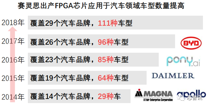
FPGA giants are optimistic about the autonomous driving track. By the end of 2018, the global automotive semiconductor industry market size approached 40 billion USD, among which FPGA applications in the automotive semiconductor field account for only about 2.5%. Autonomous driving systems impose higher requirements on in-vehicle chips, expanding the demand for main control chips from traditional GPUs to ASICs, FPGAs, and other chip types.
Currently, FPGA chips are maturing in applications within in-vehicle cameras, sensors, and other hardware devices. Additionally, due to programming flexibility, FPGA chips are widely used in the field of LiDAR. Autonomous driving vehicles heavily rely on hardware devices such as sensors and cameras, as well as software systems like in-vehicle networks, leading to a significant demand for FPGA chips. Leading FPGA manufacturers (such as Xilinx) are seizing the intelligent driving track, gradually increasing cooperation with automotive companies and vehicle networking companies. By the end of 2018, Xilinx FPGA solutions had been embedded in 111 vehicle models.
Growth of FPGA Chip Downstream Application Market Scale: In 2018, communication, consumer electronics, and automotive scenarios constituted over 80% of the total demand for global FPGA chips, and the market scale continues to expand. FPGA devices, as core components of 5G base stations, automotive terminal devices, and edge computing devices, have significant acceleration effects and face certain incremental demand in the downstream market. With the strengthening of midstream domestic enterprises, domestic FPGA chip products may enter the downstream market with a price advantage, reducing the procurement costs of downstream enterprises for high-end programmable devices.
4. Market Scale of China’s FPGA Chip Industry
The demand for FPGA chips continues to rise in application scenarios, with the development of 5G and artificial intelligence technologies promoting the expansion of China’s FPGA market and stimulating the release of incremental demand.
1. Market Scale of the FPGA Chip Industry
As the downstream application market expands, the market scale of China’s FPGA industry continues to rise. In 2018, the FPGA market scale in China approached 14 billion yuan. The development of new 5G communication technologies and machine learning technologies will further stimulate the expansion of China’s FPGA market. It is expected that by 2023, the market scale of China’s FPGA chip market will approach 46 billion yuan.
Global FPGA Market Scale Potential Will Be Released, Mainly Benefiting From the Following Factors:
Downstream application scenarios are becoming increasingly diverse: FPGA chips are more flexible than ASICs, saving tape-out time costs and shortening time to market. The application scenarios have expanded from communication transceivers and consumer electronics to automotive electronics, data centers, high-performance computing, industrial vision, and medical testing. In the short term, the Chinese FPGA application scenarios remain dispersed, with both stock and incremental markets having room for expansion.
Some application scenarios are irreplaceable: FPGA chips have advantages in low R&D costs and manufacturing costs in scenarios where technology is unstable, flexibility is highly demanded, and demand volumes are small (devices can be programmed on-site according to specific needs).
Global Market Share Analysis:
The Asia-Pacific market demand is significant. The Asia-Pacific region is the main application market for FPGAs, accounting for over 40% of the global market share. By the end of 2018, China’s FPGA market scale approached 14 billion yuan, facing significant incremental demand space with the expansion of 5G communication infrastructure.
North American giants dominate the top market. In North America, Xilinx and Intel (acquiring Altera) maintain a duopoly in the FPGA market. In the Chinese FPGA market, Xilinx holds over 50% market share, while Intel’s share is close to 30%.
5. The Complexity of FPGA Chip Design Continues to Increase
From 2016 to 2018, the proportion of high-performance, high-security programmable chip design projects in the global FPGA R&D field increased, leading to an increase in FPGA design complexity.
The demand for security features has increased, raising the complexity of high-performance FPGA chip designs.
Increase in Security Critical Standards and Guidelines:
The increase in demand for security features can be expressed by the increase in security critical standards and guidelines. In 2016 and prior, most FPGA development projects were based on a single security critical standard, while from 2018 onwards, more FPGA R&D projects are developed based on one or more security critical standards and guidelines.
Increase in Security Assurance Hardware Module Design Projects:
Security assurance hardware module designs are widely used in areas such as encryption keys, digital rights management keys, passwords, and biometric reference data. Compared to 2016, the proportion of global FPGA security feature module design projects significantly increased in 2018 (with an increase of over 5%). The enhancement of security features increases the demand for design verification and verification complexity.
Other Design Projects Increase Chip Verification Complexity:
1. Increase in the Number of Embedded Processor Cores: Compared to 2016, more FPGA designs in 2018 tend towards SoC-class designs. In 2018, over 40% of FPGA designs included 2 or more embedded processors, and nearly 15% included 4 or more embedded processors, increasing the complexity of verification processes.
2. Increase in the Number of Asynchronous Clock Domains: In 2018, about 90% of FPGA design projects included 2 or more asynchronous clock domains, increasing the verification workload (verification models tend to be complex, and code exceptions increase).
6. Application Scenarios and Market Demand
1. Widely Used in Machine Learning Reinforcement Projects
FPGA chips are more suitable for non-fixed, non-standard machine learning evolutionary environments.
FPGA performs excellently in machine learning. Performance comparisons can refer to Xilinx’s public test results, which compare the performance of the reVISION series FPGA chips with NVIDIA’s Tegra X1 series GPU chips in the field of machine learning. Data shows that the FPGA solution outperforms the GPU solution by 6 times in terms of image capture speed per unit power consumption and by 42 times in frame rate for computer vision processing, while the FPGA’s latency is 1/5 that of the GPU. Comparing Xilinx FPGA with Intel’s Arria 10 SoC series CPU devices, Xilinx FPGA devices can enhance deep learning and computer vision computational efficiency by 3 to 7 times.
Companies Adopting New Architectures (Visual Data Transmission to FPGA Accelerates Edge Server Clusters):
FPGA optimizes stream processing. FPGA solutions can optimize stream processing for video analysis and deep learning inference (one of the big data processing techniques). Based on their flexible programming characteristics, FPGA solutions can meet reconfiguration needs, suitable for general models such as inventory management, fraud control, facial recognition, as well as complex models such as tracking, natural language interaction, and emotional detection.
Startups actively adopt FPGA solutions. Startups like Megh Computing and PointR.ai are actively adopting FPGA solutions to establish new video data processing architectures, leveraging compact, low-power computing module advantages.
△Source: Wilson Research Group and Mentor, edited by Leopard Research Institute
2. 5G Communication System Construction Increases Demand for FPGA Chips
The communication scenario is the most widely used application scenario for FPGA chips in the downstream of the industry chain (accounting for about 40%). With the development of 5G communication technology and hardware equipment upgrades (innovation in base station antenna transceivers), FPGA faces strong market demand drivers.
5G communication is about to be commercially scaled, driving an increase in FPGA chip usage and price release space.
New Base Station Antenna Transceivers Use FPGA Chips. Under the Massive MIMO base station technology conditions of the 5G era, the number of base station transceiver channels has increased from 16T16R (dual-mode solution) to a maximum of 128T128R, and FPGA chips can be used to achieve multi-channel signal beamforming. For example, the mid-frequency and baseband subsystems of a 64-channel millimeter-wave MIMO full DBF transceiver use Xilinx Kintex-7 series FPGA. The mid-frequency and baseband subsystems together achieve general wireless access functionality.
Industry experts with over 10 years of product development and algorithm research experience in the FPGA chip industry indicate that FPGA has advantages over CPU and GPU in terms of power consumption and computational speed. Communication equipment companies will increase the application of FPGA devices in core equipment such as base station antenna transceivers (for example, leading mobile communication equipment manufacturers like Jingxin Communication embed FPGA chips in new transceiver products).
The global FPGA communication market is growing rapidly. By the end of 2018, the global FPGA communication market accounted for nearly 45% of the application market. From 2020 to 2025, the global FPGA communication market scale is expected to have a compound annual growth rate of nearly 10%.
5G infrastructure will use FPGA devices as core components. The growth of the 5G communication market is certain. Related infrastructures (data centers, macro stations, micro stations, etc.) penetrate into various fields such as the Internet of Things and edge computing, with 5G infrastructure projects using FPGA as core components, driving an increase in FPGA price release space.
In the next 10 years, the number of small base stations may exceed 10,000, driving an increase in FPGA device usage.
Currently, the average price of FPGA used in base stations is below 100 yuan, but factors such as increased technical complexity are pushing prices higher (>100 yuan).
3. The Scale Commercialization of Autonomous Driving Increases Demand for FPGA
FPGA giants are optimistic about the autonomous driving track. By the end of 2018, the global automotive semiconductor industry market size approached 40 billion USD, among which FPGA applications in the automotive semiconductor field account for only about 2.5%. Autonomous driving systems impose higher requirements on in-vehicle chips, expanding the demand for main control chips from traditional GPUs to ASICs, FPGAs, and other chip types.
Currently, FPGA chips are maturing in applications within in-vehicle cameras, sensors, and other hardware devices. Additionally, due to programming flexibility, FPGA chips are widely used in the field of LiDAR. Autonomous driving vehicles heavily rely on hardware devices such as sensors and cameras, as well as software systems like in-vehicle networks, leading to a significant demand for FPGA chips. Leading FPGA manufacturers (such as Xilinx) are seizing the intelligent driving track, gradually increasing cooperation with automotive companies and vehicle networking companies. By the end of 2018, Xilinx FPGA solutions had been embedded in 111 vehicle models.
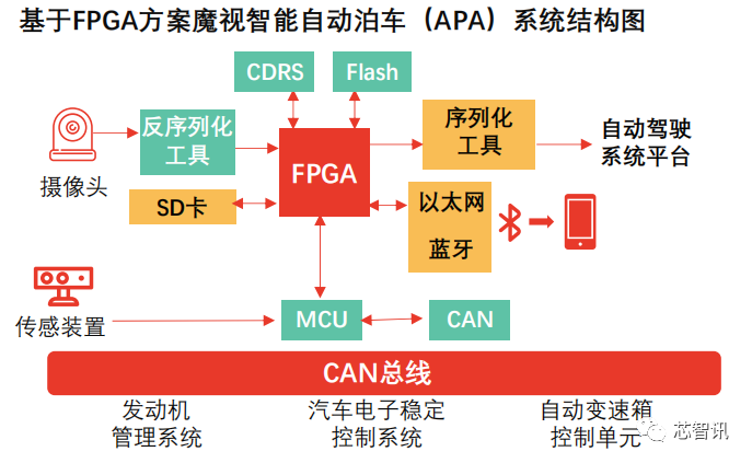
 FPGA’s application coverage in autonomous driving systems is broad. FPGA chips can be applied in ADAS systems, LiDAR, automated parking systems, motor control, in-vehicle entertainment information systems, driver information systems, and other areas, with extensive applications. For example, the MoVision intelligent automated parking system connects FPGA chips to the in-vehicle CAN bus, linking Bluetooth, SD cards, and other communication components, and connects with cameras and sensor devices through MCUs. Leading FPGA manufacturer Xilinx is actively laying out the ADAS field. In the long term, ADAS systems are becoming more complex (including front-facing cameras, driver monitoring cameras, panoramic cameras, short-range radar, and long-range LiDAR), increasing the demand for FPGA usage. By 2025, autonomous driving will enter the scale commercialization phase, continuously driving the integration of FPGAs with automotive electronics and in-vehicle software systems.
 7. Constraints on China’s FPGA Chip Industry – Lack of FPGA Design Talent Team Strength
The threshold for FPGA chip design is high (higher than that of CPUs, memory, DSP), and Chinese domestic manufacturers started late, being in the initial stage of industrial ecosystem construction, with a weak foundation in talent resource reserves.
1. Insufficient Talent Reserve in China’s FPGA Chip Design Compared to International Markets
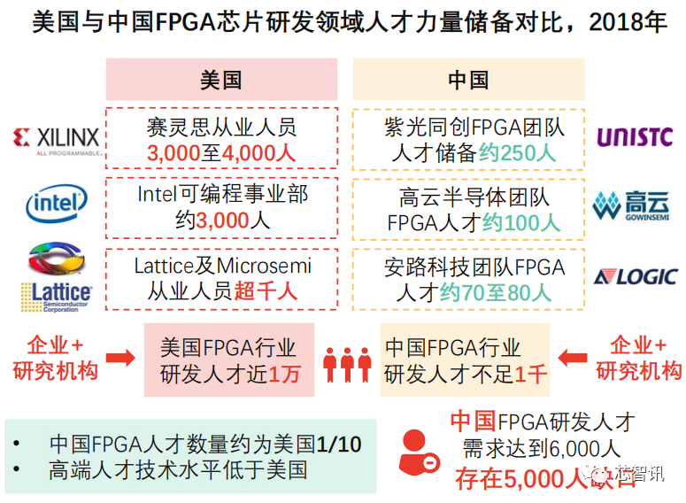
China’s FPGA talent reserve is about 1/10 of the corresponding talent reserve in the U.S. According to the “White Paper on Talent in China’s Integrated Circuit Industry” published by the China International Talent Exchange Foundation and other organizations, by the end of 2018, the stock talent in China’s integrated circuit industry was about 400,000 people, while the industry’s talent demand is expected to exceed 700,000 by 2020, resulting in a talent gap of over 300,000 people. In the FPGA sector, leading foreign manufacturers such as Intel, Xilinx, Lattice, and related universities and research institutions have nearly 10,000 relevant talents. In contrast, China is lacking in FPGA design and R&D talents, with leading manufacturers such as Unisoc, Hygon Semiconductor, and Anlu Technology having an average of fewer than 200 R&D personnel, and the overall industry talent team is insufficient, with fewer than 1,000 people, which becomes a core factor restricting the technological development and product upgrades of China’s FPGA chip industry.
2. Late Start of Industry Development and Lack of Industry-Academia-Research Collaboration
The Chinese FPGA industry started in 2000, while the U.S. has had a background of R&D starting as early as the 1980s. In 2010, China achieved mass production of FPGA chips. U.S. universities closely collaborate with chip manufacturers, transferring a large amount of technology to enterprises. In contrast, Chinese companies lack experience in cooperation with universities and research institutions, resulting in insufficient industry-academia-research collaboration, with most existing core talents in the industry being imported from overseas.
3. Lack of R&D Strength Restricts Enterprise Growth
Global leading FPGA manufacturers rely on patent technology accumulation and talent cultivation, along with a 20-year head start in development compared to Chinese enterprises, firmly occupying the first-tier camp globally. The high entry barrier of the FPGA industry makes it difficult for Chinese leading companies to gain a latecomer advantage. Currently, Xilinx has entered the R&D stage of 7nm process billion-gate high-end FPGA products, while leading Chinese manufacturers such as Unisoc and Hygon Semiconductor have initiated R&D work on 28nm process tens of millions of gates (70 million) mid-to-high-density FPGAs, lagging about 2 to 3 generations behind global top levels, urgently needing talent resource support.
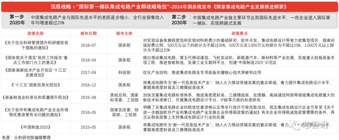
8. Policies and Regulations of China’s FPGA Chip Industry – Policy Analysis
To further guide the orderly development of the FPGA industry and highlight the strategic position of the integrated circuit industry, national policy departments are integrating industry, market, and user resources, creating a policy foundation for Chinese integrated circuit enterprises to develop towards the international first tier.
Since the 12th Five-Year Plan, the country has emphasized the position of the integrated circuit industry as a leading industry, placing greater importance on the role of chip technology development in promoting the transformation and upgrading of industrial manufacturing and information technology development. The state has introduced multiple favorable policies from the perspectives of market demand, supply, industry chain structure, and value chain.
9. Global FPGA Market Competitive Landscape
The global FPGA chip market is highly concentrated, with leading manufacturers occupying the “air supremacy.” New entrants provide momentum for industry development through product innovation, while intelligent market demand may push FPGA technology into the mainstream.
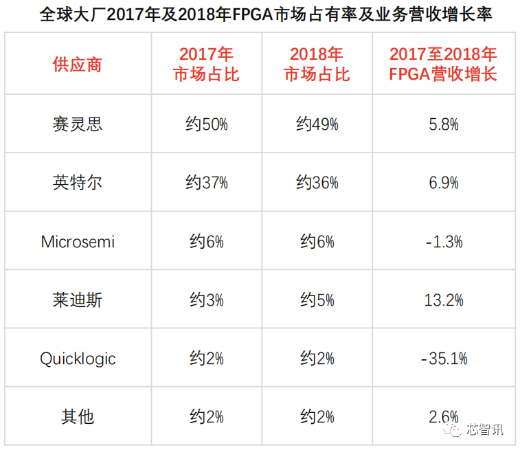
The global FPGA market is monopolized by four giants: Xilinx, Intel (acquiring Altera), Lattice, and Microsemi, which monopolize over 9,000 patent technologies and hold the industry’s “air supremacy.”
By the end of 2018, the global FPGA market was dominated by Xilinx (49% market share), Intel (Altera) with over 30%, and Lattice and Microsemi each occupying over 5% of the global market scale. In contrast, Chinese manufacturers collectively hold less than 3% of the global FPGA market share.
Since the establishment of the FPGA chip industry, over 70 companies have participated in global competition, with new startups emerging (such as Achronix Semiconductor and MathStar). Product innovation provides momentum for industry development, with the speed of innovation for new programmable logic devices (analog nature) accelerating, such as Cypress Semiconductor’s development of configurable mixed-signal circuits PSoC (Programmable System on Chip) and Actel’s launch of Fusion (programmable mixed-signal chips). Additionally, some startups have launched Field Programmable Analog Arrays (FPAAs).
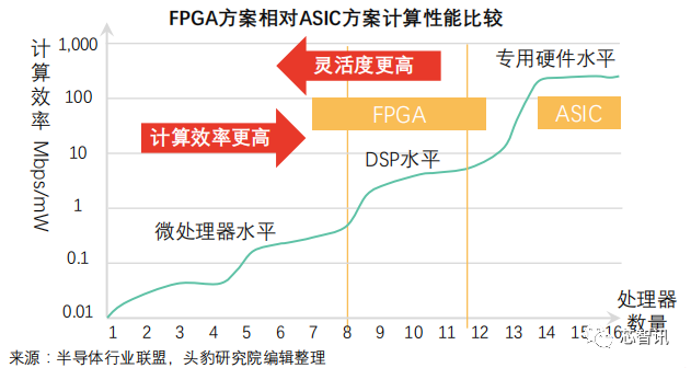
As the intelligent market demand evolves, highly customized chips (SoC ASIC) face increasing market risks due to their large non-repetitive investment scale and long R&D cycles. In contrast, FPGA has advantages in parallel computing tasks and can replace some ASICs in high-performance, multi-channel fields. The demand for multi-channel computing tasks in artificial intelligence drives FPGA technology towards the mainstream.
Based on the advantages of FPGA chips in small batch production (with a tape-out threshold of 50,000 chips) and multi-channel computing specialized equipment (radar, aerospace devices), some downstream application markets are replacing ASIC application solutions with FPGA.
International Competitive Landscape: The global FPGA market was initially highly monopolized by two U.S. giants (Xilinx and Altera). Following a series of market mergers and acquisitions and the influence of startup teams, the first-tier international market camp has expanded (including Xilinx, Intel, Lattice, Microsemi, Achronix, Flexlogic, Quicklogic, etc.).
7. Constraints on China’s FPGA Chip Industry – Lack of FPGA Design Talent Team Strength
The threshold for FPGA chip design is high (higher than that of CPUs, memory, DSP), and Chinese domestic manufacturers started late, being in the initial stage of industrial ecosystem construction, with a weak foundation in talent resource reserves.
1. Insufficient Talent Reserve in China’s FPGA Chip Design Compared to International Markets
China’s FPGA talent reserve is about 1/10 of the corresponding talent reserve in the U.S. According to the “White Paper on Talent in China’s Integrated Circuit Industry” published by the China International Talent Exchange Foundation and other organizations, by the end of 2018, the stock talent in China’s integrated circuit industry was about 400,000 people, while the industry’s talent demand is expected to exceed 700,000 by 2020, resulting in a talent gap of over 300,000 people. In the FPGA sector, leading foreign manufacturers such as Intel, Xilinx, Lattice, and related universities and research institutions have nearly 10,000 relevant talents. In contrast, China is lacking in FPGA design and R&D talents, with leading manufacturers such as Unisoc, Hygon Semiconductor, and Anlu Technology having an average of fewer than 200 R&D personnel, and the overall industry talent team is insufficient, with fewer than 1,000 people, which becomes a core factor restricting the technological development and product upgrades of China’s FPGA chip industry.
2. Late Start of Industry Development and Lack of Industry-Academia-Research Collaboration
The Chinese FPGA industry started in 2000, while the U.S. has had a background of R&D starting as early as the 1980s. In 2010, China achieved mass production of FPGA chips. U.S. universities closely collaborate with chip manufacturers, transferring a large amount of technology to enterprises. In contrast, Chinese companies lack experience in cooperation with universities and research institutions, resulting in insufficient industry-academia-research collaboration, with most existing core talents in the industry being imported from overseas.
3. Lack of R&D Strength Restricts Enterprise Growth
Global leading FPGA manufacturers rely on patent technology accumulation and talent cultivation, along with a 20-year head start in development compared to Chinese enterprises, firmly occupying the first-tier camp globally. The high entry barrier of the FPGA industry makes it difficult for Chinese leading companies to gain a latecomer advantage. Currently, Xilinx has entered the R&D stage of 7nm process billion-gate high-end FPGA products, while leading Chinese manufacturers such as Unisoc and Hygon Semiconductor have initiated R&D work on 28nm process tens of millions of gates (70 million) mid-to-high-density FPGAs, lagging about 2 to 3 generations behind global top levels, urgently needing talent resource support.
8. Policies and Regulations of China’s FPGA Chip Industry – Policy Analysis
To further guide the orderly development of the FPGA industry and highlight the strategic position of the integrated circuit industry, national policy departments are integrating industry, market, and user resources, creating a policy foundation for Chinese integrated circuit enterprises to develop towards the international first tier.
Since the 12th Five-Year Plan, the country has emphasized the position of the integrated circuit industry as a leading industry, placing greater importance on the role of chip technology development in promoting the transformation and upgrading of industrial manufacturing and information technology development. The state has introduced multiple favorable policies from the perspectives of market demand, supply, industry chain structure, and value chain.
9. Global FPGA Market Competitive Landscape
The global FPGA chip market is highly concentrated, with leading manufacturers occupying the “air supremacy.” New entrants provide momentum for industry development through product innovation, while intelligent market demand may push FPGA technology into the mainstream.
The global FPGA market is monopolized by four giants: Xilinx, Intel (acquiring Altera), Lattice, and Microsemi, which monopolize over 9,000 patent technologies and hold the industry’s “air supremacy.”
By the end of 2018, the global FPGA market was dominated by Xilinx (49% market share), Intel (Altera) with over 30%, and Lattice and Microsemi each occupying over 5% of the global market scale. In contrast, Chinese manufacturers collectively hold less than 3% of the global FPGA market share.
Since the establishment of the FPGA chip industry, over 70 companies have participated in global competition, with new startups emerging (such as Achronix Semiconductor and MathStar). Product innovation provides momentum for industry development, with the speed of innovation for new programmable logic devices (analog nature) accelerating, such as Cypress Semiconductor’s development of configurable mixed-signal circuits PSoC (Programmable System on Chip) and Actel’s launch of Fusion (programmable mixed-signal chips). Additionally, some startups have launched Field Programmable Analog Arrays (FPAAs).
As the intelligent market demand evolves, highly customized chips (SoC ASIC) face increasing market risks due to their large non-repetitive investment scale and long R&D cycles. In contrast, FPGA has advantages in parallel computing tasks and can replace some ASICs in high-performance, multi-channel fields. The demand for multi-channel computing tasks in artificial intelligence drives FPGA technology towards the mainstream.
Based on the advantages of FPGA chips in small batch production (with a tape-out threshold of 50,000 chips) and multi-channel computing specialized equipment (radar, aerospace devices), some downstream application markets are replacing ASIC application solutions with FPGA.
International Competitive Landscape: The global FPGA market was initially highly monopolized by two U.S. giants (Xilinx and Altera). Following a series of market mergers and acquisitions and the influence of startup teams, the first-tier international market camp has expanded (including Xilinx, Intel, Lattice, Microsemi, Achronix, Flexlogic, Quicklogic, etc.).
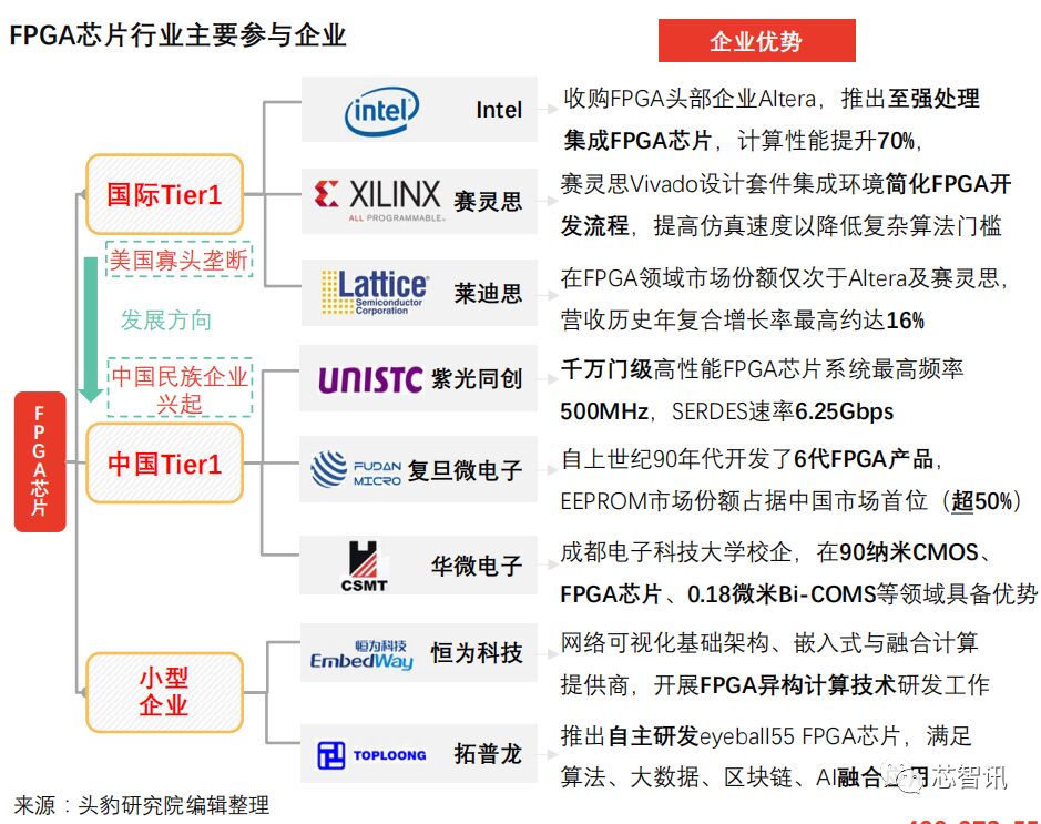 Chinese FPGA Manufacturers: Chinese FPGA chip R&D enterprises can be exemplified by Unisoc, Guowei Electronics, Chengdu Huayi Electronics, Anlu Technology, Zhi Duo Jing, Gao Yun Semiconductor, Shanghai Fudan Microelectronics, and Jingwei Qili. From a product perspective, the performance indicators of Chinese FPGA hardware lag significantly behind those of Xilinx and Intel. Unisoc is currently the only company in the Chinese market with the capability for independent research and development and manufacturing of high-performance billion-gate FPGAs. Shanghai Fudan Microelectronics launched self-owned intellectual property billion-gate FPGA products in May 2018. Chinese FPGA companies are closely following the steps of major manufacturers, laying out markets in artificial intelligence, autonomous driving, etc., and building a complete product line across high, medium, and low ends.
Breakthrough Points for Chinese FPGA Enterprises: Currently, the chip design software and application software of Chinese FPGA manufacturers are not unified, leading to resource wastage at the client end. Leading manufacturers can take the lead in concentrating industry chain resources to enhance the overall competitiveness of the industry.
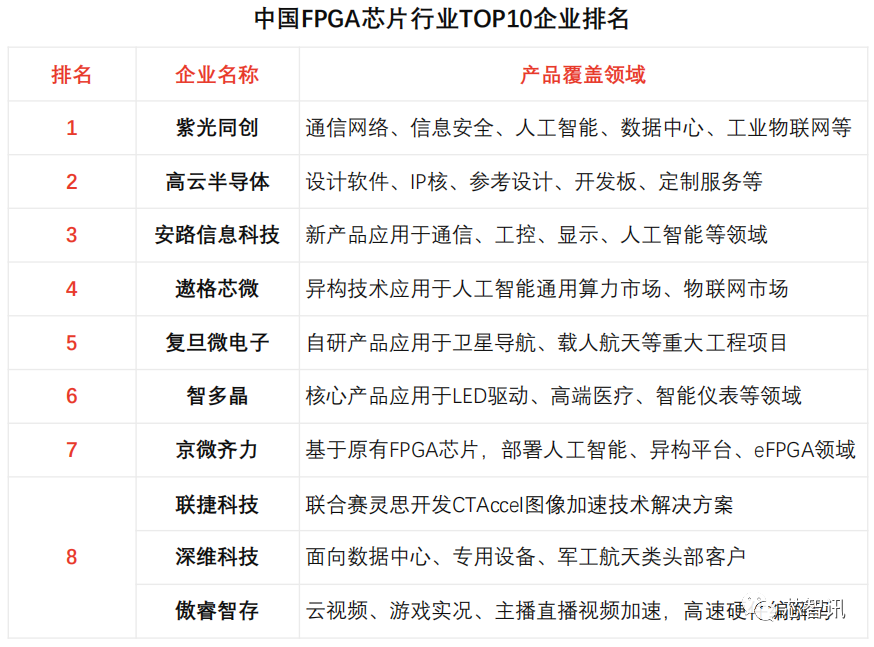
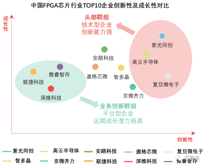
10. Top 10 Enterprises in China’s FPGA Chip Industry
Competition subjects in China’s FPGA chip industry include R&D enterprises and application solution providers. With the rapid development of artificial intelligence, the Internet of Things, and 5G technologies, Chinese FPGA manufacturers are ushering in the best market entry period.
Characteristics of Chinese FPGA Manufacturers: The FPGA chip industry competition is highly concentrated, with most Chinese FPGA manufacturers focusing on 40nm and 55nm product series, lacking competitiveness in both the Chinese and global markets compared to Xilinx and Intel (manufacturing processes, scale capacity, software capabilities are all at a disadvantage). Chinese manufacturers urgently need to seek breakthrough paths in a highly concentrated market. In 2017, the telecommunications industry’s demand accelerated the domestic FPGA chip localization process, but many Chinese manufacturers adopted a “low-price competition” strategy, failing to achieve healthy and sustainable competition.
Chinese manufacturers can break through competitive bottlenecks from two aspects: transitioning FPGA manufacturing processes from 28nm to 16nm, and approaching the internationally leading level of 7nm, while transitioning chip logic unit scales from 500K to 1M and 2M, potentially challenging 3D chip technology in the long term. Manufacturers can rely on testability design, reliability design, high testing standards, and mass production management to break through quality bottlenecks, adopting a “technology + product + management” strategy to win.
Chip development enterprises: Chinese FPGA R&D enterprises can be exemplified by Jingwei Qili, Fudan Microelectronics, Unisoc, Gao Yun Semiconductor, Anlu Technology, Zhi Duo Jing, etc.
Application solution enterprises: Application solution providers can be exemplified by Lianjie Technology, Shenwei Technology, and Aoruizhi Storage.
Characteristics of Top 10 Enterprises:
Top 10 enterprises in China’s FPGA chip industry are gradually promoting the localization process of FPGA technology. Due to factors such as manufacturing capabilities, packaging and testing processes, and IP resources, the technological innovation strength of Chinese FPGA chip companies urgently needs to be improved.
Unisoc: Launched self-owned intellectual property large-scale FPGA development software Pango DesignSuite, supporting the design and development of tens of millions of gates FPGA devices.
Gao Yun Semiconductor: Launched China’s first 55nm embedded Flash SRAM non-volatile FPGA chip, achieving seamless connection between programmable logic devices and embedded processors.
Anlu Technology: Engaged in R&D of 28nm and 12nm tens of millions of gates and 50 million gates FPGAs and SoCFPGA, independently developing a complete system from HDL description to on-chip debugging.
Aogexin Microelectronics: Launched China’s first general-purpose FPGA product series, maintaining high compatibility in software and hardware pin packaging, supporting low, medium, and high-end embedded applications and upgrades.
Fudan Microelectronics: Integrated dedicated ultra-high-speed serial-parallel conversion modules, highly flexible configurable modules, and other applicable billion-gate FPGA application module circuits.
Zhi Duo Jing: Achieved mass production of mid-density FPGAs with 55nm and 40nm processes, independently developed FPGA development software “HqFpga”, supporting layout, routing, timing analysis, and internal logic analysis tasks.
Jingwei Qili: Utilized 40nm process chips in the smart wearable device field, possessing over 100 FPGA patents and proprietary technology (international patents) authorization and secondary development rights.
Lianjie Technology: Developed CNN-based image analysis technology, launching FPGA acceleration solutions that can double the speed of neural network-based facial recognition.
Shenwei Technology: Focused on FPGA AI application development, with a team possessing experience from Cadence, IBM, and the Chinese Academy of Sciences, giving them an advantage in product engineering capabilities.
Aoruizhi Storage: Provides new FPGA video transcoding services, supporting deep learning applications without changing or adding hardware.
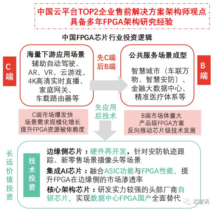
11. Expert Opinions – Investment Logic and Risk Overview of China’s FPGA Chip Industry
Experts suggest that within the next five years, investment teams focus on China’s FPGA market based on the investment logic of first C-end then B-end, first application scenarios then technology development, and first product-level then chip-level funding injection.
From C-end to B-end: The C-end market (application side) in China is likely to produce explosive products, with short-term high-definition cloud gaming and video likely to create numerous application scenarios. As the number of user-end application scenarios increases, the dependency of devices on underlying computing resources rises, leading to rapid market scale expansion. Experts suggest that investment teams seek investment opportunities in sub-scenarios with landing value (financial big data analysis, image video processing, gene sequencing, precision medicine, voice recognition, image recognition, etc.). After the maturity of C-end applications, investment teams can focus on B-end needs, where the invested objects can integrate solutions, FPGA third-party products, and independently develop PaaS platforms to provide productized services for bank clients, government clients, etc.
From Scenarios to Technology: The underlying technology R&D difficulty of FPGA chips is high and requires significant investment. Experts suggest that investment teams gradually transition from scenario investments to technology investments, with technology investment approaches referencing the R&D models of companies like Hikvision, Dahua, and Deep Insight Technology. These companies utilize the semi-customized basis of FPGA to create edge-side chips (focusing on facial recognition, security trajectory tracking, new retail scenario cameras, etc.), with this technology being redeveloped based on existing hardware, presenting lower investment risks compared to fundamental technology R&D.
In chip R&D, startup companies without major manufacturer support are likely to face funding and technical dilemmas.
Avoid purchasing a large amount of FPGA hardware: Investment objects can use FPGA cloud services provided by data centers such as Alibaba Cloud and Tencent Cloud.
Seek government funding support: For instance, under government funding support, a cloud rendering data center in Xinjiang has deployed a large number of GPU and FPGA foundational hardware.
Deeply explore the functional characteristics of application scenarios: Companies unable to rapidly enhance competitiveness in the short term can launch dedicated FPGA chips for specific scenarios, only outputting algorithms, and releasing chips through foundries, providing board solutions with targeted functional characteristics after market validation in application scenarios.
Chinese FPGA Manufacturers: Chinese FPGA chip R&D enterprises can be exemplified by Unisoc, Guowei Electronics, Chengdu Huayi Electronics, Anlu Technology, Zhi Duo Jing, Gao Yun Semiconductor, Shanghai Fudan Microelectronics, and Jingwei Qili. From a product perspective, the performance indicators of Chinese FPGA hardware lag significantly behind those of Xilinx and Intel. Unisoc is currently the only company in the Chinese market with the capability for independent research and development and manufacturing of high-performance billion-gate FPGAs. Shanghai Fudan Microelectronics launched self-owned intellectual property billion-gate FPGA products in May 2018. Chinese FPGA companies are closely following the steps of major manufacturers, laying out markets in artificial intelligence, autonomous driving, etc., and building a complete product line across high, medium, and low ends.
Breakthrough Points for Chinese FPGA Enterprises: Currently, the chip design software and application software of Chinese FPGA manufacturers are not unified, leading to resource wastage at the client end. Leading manufacturers can take the lead in concentrating industry chain resources to enhance the overall competitiveness of the industry.
10. Top 10 Enterprises in China’s FPGA Chip Industry
Competition subjects in China’s FPGA chip industry include R&D enterprises and application solution providers. With the rapid development of artificial intelligence, the Internet of Things, and 5G technologies, Chinese FPGA manufacturers are ushering in the best market entry period.
Characteristics of Chinese FPGA Manufacturers: The FPGA chip industry competition is highly concentrated, with most Chinese FPGA manufacturers focusing on 40nm and 55nm product series, lacking competitiveness in both the Chinese and global markets compared to Xilinx and Intel (manufacturing processes, scale capacity, software capabilities are all at a disadvantage). Chinese manufacturers urgently need to seek breakthrough paths in a highly concentrated market. In 2017, the telecommunications industry’s demand accelerated the domestic FPGA chip localization process, but many Chinese manufacturers adopted a “low-price competition” strategy, failing to achieve healthy and sustainable competition.
Chinese manufacturers can break through competitive bottlenecks from two aspects: transitioning FPGA manufacturing processes from 28nm to 16nm, and approaching the internationally leading level of 7nm, while transitioning chip logic unit scales from 500K to 1M and 2M, potentially challenging 3D chip technology in the long term. Manufacturers can rely on testability design, reliability design, high testing standards, and mass production management to break through quality bottlenecks, adopting a “technology + product + management” strategy to win.
Chip development enterprises: Chinese FPGA R&D enterprises can be exemplified by Jingwei Qili, Fudan Microelectronics, Unisoc, Gao Yun Semiconductor, Anlu Technology, Zhi Duo Jing, etc.
Application solution enterprises: Application solution providers can be exemplified by Lianjie Technology, Shenwei Technology, and Aoruizhi Storage.
Characteristics of Top 10 Enterprises:
Top 10 enterprises in China’s FPGA chip industry are gradually promoting the localization process of FPGA technology. Due to factors such as manufacturing capabilities, packaging and testing processes, and IP resources, the technological innovation strength of Chinese FPGA chip companies urgently needs to be improved.
Unisoc: Launched self-owned intellectual property large-scale FPGA development software Pango DesignSuite, supporting the design and development of tens of millions of gates FPGA devices.
Gao Yun Semiconductor: Launched China’s first 55nm embedded Flash SRAM non-volatile FPGA chip, achieving seamless connection between programmable logic devices and embedded processors.
Anlu Technology: Engaged in R&D of 28nm and 12nm tens of millions of gates and 50 million gates FPGAs and SoCFPGA, independently developing a complete system from HDL description to on-chip debugging.
Aogexin Microelectronics: Launched China’s first general-purpose FPGA product series, maintaining high compatibility in software and hardware pin packaging, supporting low, medium, and high-end embedded applications and upgrades.
Fudan Microelectronics: Integrated dedicated ultra-high-speed serial-parallel conversion modules, highly flexible configurable modules, and other applicable billion-gate FPGA application module circuits.
Zhi Duo Jing: Achieved mass production of mid-density FPGAs with 55nm and 40nm processes, independently developed FPGA development software “HqFpga”, supporting layout, routing, timing analysis, and internal logic analysis tasks.
Jingwei Qili: Utilized 40nm process chips in the smart wearable device field, possessing over 100 FPGA patents and proprietary technology (international patents) authorization and secondary development rights.
Lianjie Technology: Developed CNN-based image analysis technology, launching FPGA acceleration solutions that can double the speed of neural network-based facial recognition.
Shenwei Technology: Focused on FPGA AI application development, with a team possessing experience from Cadence, IBM, and the Chinese Academy of Sciences, giving them an advantage in product engineering capabilities.
Aoruizhi Storage: Provides new FPGA video transcoding services, supporting deep learning applications without changing or adding hardware.
11. Expert Opinions – Investment Logic and Risk Overview of China’s FPGA Chip Industry
Experts suggest that within the next five years, investment teams focus on China’s FPGA market based on the investment logic of first C-end then B-end, first application scenarios then technology development, and first product-level then chip-level funding injection.
From C-end to B-end: The C-end market (application side) in China is likely to produce explosive products, with short-term high-definition cloud gaming and video likely to create numerous application scenarios. As the number of user-end application scenarios increases, the dependency of devices on underlying computing resources rises, leading to rapid market scale expansion. Experts suggest that investment teams seek investment opportunities in sub-scenarios with landing value (financial big data analysis, image video processing, gene sequencing, precision medicine, voice recognition, image recognition, etc.). After the maturity of C-end applications, investment teams can focus on B-end needs, where the invested objects can integrate solutions, FPGA third-party products, and independently develop PaaS platforms to provide productized services for bank clients, government clients, etc.
From Scenarios to Technology: The underlying technology R&D difficulty of FPGA chips is high and requires significant investment. Experts suggest that investment teams gradually transition from scenario investments to technology investments, with technology investment approaches referencing the R&D models of companies like Hikvision, Dahua, and Deep Insight Technology. These companies utilize the semi-customized basis of FPGA to create edge-side chips (focusing on facial recognition, security trajectory tracking, new retail scenario cameras, etc.), with this technology being redeveloped based on existing hardware, presenting lower investment risks compared to fundamental technology R&D.
In chip R&D, startup companies without major manufacturer support are likely to face funding and technical dilemmas.
Avoid purchasing a large amount of FPGA hardware: Investment objects can use FPGA cloud services provided by data centers such as Alibaba Cloud and Tencent Cloud.
Seek government funding support: For instance, under government funding support, a cloud rendering data center in Xinjiang has deployed a large number of GPU and FPGA foundational hardware.
Deeply explore the functional characteristics of application scenarios: Companies unable to rapidly enhance competitiveness in the short term can launch dedicated FPGA chips for specific scenarios, only outputting algorithms, and releasing chips through foundries, providing board solutions with targeted functional characteristics after market validation in application scenarios.