
Which is better, ASIC or FPGA? What are the differences in their processes? Is it necessary to switch from FPGA to ASIC design? Various questions about ASIC and FPGA are frequently seen online.
ASIC (Application Specific Integrated Circuit) refers to integrated circuits designed and manufactured to meet specific user requirements and the needs of specific electronic systems.
FPGA (Field Programmable Gate Array) is a product that has further developed based on programmable devices such as PAL (Programmable Array Logic) and GAL (Generic Array Logic). FPGA is a chip that can reconfigure its circuits, representing a hardware-reconfigurable architecture that can change its application scenarios at any time through programming.
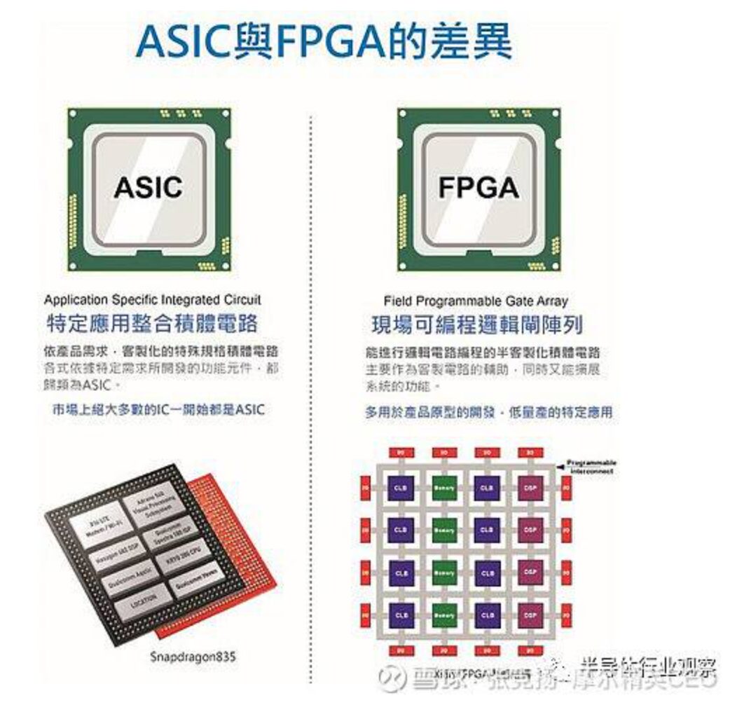
Image source: Internet
Similarities and Differences Between FPGA and ASIC
Similarities: Essentially, both are chips. FPGA development strictly follows the ASIC development process, and both are in the direction of integrated circuits. Generally speaking, if an electronic hardware product can be made with FPGA, it can also be made with ASIC, and the products produced through the two different channels can achieve the same functionality.
Differences: The former downloads the completed netlist or circuit code into the FPGA, forming a gate array. If issues are found during product delivery or usage, patches can be reapplied, and versions can be updated to proceed normally. In contrast, ASIC must go through the process of wafer fabrication to become a chip, which has higher requirements! The design process is very lengthy, generally taking about a year, requiring multiple verification engineers, because once a problem occurs later, it can only be re-manufactured, leading to many or serious bugs, and there is even a risk of total recall, potentially resulting in financial losses.
In the ASIC design process, FPGA is often used for prototype verification. Completing FPGA verification can be said to complete 50-70% of the entire ASIC process.
Differences in Design Processes of FPGA and ASIC
FPGA design has the capability of reconfigurable chips, while ASIC design generally has fewer reconfigurable chip functions.
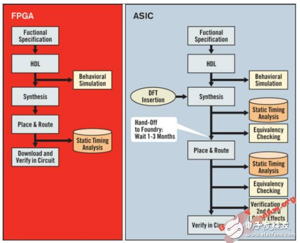
FPGA is also known as the “universal chip”, containing a large number of configurable units (based on LUT slices), configurable IPs (DSP, CMT, PCIe, Serdes, etc.), and configurable memory. Users can download their designs to the FPGA chip to quickly realize their functions, allowing for rapid demo system construction and a short design cycle.
ASIC chips must first go through complex design processes such as code design, synthesis, and back-end processing, followed by several months of production, processing, and packaging testing before obtaining the chip to build the system. The complexity arises because, in addition to ensuring functionality, various power consumption and area requirements must be optimized, resulting in a long overall design cycle.
Choosing the Right Design Based on Different Situations
Considering time constraints, the ASIC design process is lengthy, typically taking about a year, while FPGA design can generally be completed in a few weeks or one to two months. If you want to see results quickly, choosing FPGA design is preferable.
In terms of performance, chips designed with ASIC tend to be better, as they are fully customized and offer more stable performance. ASIC (Application Specific Integrated Circuit) itself is a type of dedicated integrated circuit chip. To use a vivid analogy, if a movie company wants to create a model of Master Yoda, option one is to buy a few boxes of LEGO bricks and quickly solve the problem by building with them. Option two is to contact a mold factory, draw blueprints, and mass-produce. FPGA design results in a Yoda model built from LEGO bricks, while ASIC design results in a finalized Yoda model, which is more stable.

Regarding design costs, ASIC design generally costs millions to hundreds of millions, but if the production volume is high, the cost per ASIC chip can be low, with particularly cheap chips costing around 2 dollars; while FPGA design can sometimes be completed for a few hundred dollars, but if the production volume is high, the cost per unit remains significant, leading to substantial expenses. Therefore, for small batch production and usage, FPGA design holds advantages, while ASIC is advantageous for large-scale production and usage.
In fact, many domestic companies initially used FPGA design when market development was still unstable; only after gaining a certain market presence and risk tolerance did they start using ASIC design.
Is It Necessary for FPGA Engineers to Transition to ASIC Design Engineers?
Although the FPGA engineering market is currently developing well, many are considering transitioning to ASIC design engineering.
On one hand, there are currently relatively more FPGA engineers in the domestic market. Many can develop their projects by purchasing an FPGA board for a few thousand dollars during their studies, creating their training environment; however, ASIC design engineers are relatively scarce because schools cannot establish a mature training environment for IC design, and many lack knowledge in this area. Thus, the question arises: is it more promising to do what most people can do or to do what only a few can do? The answer is evident.
On the other hand, based on the current situation, another clear point is that ASIC design generally offers higher salaries than FPGA design, with a much higher ceiling.
Those who originally worked with FPGA are generally familiar with Verilog, which provides a significant advantage when transitioning to ASIC. Taking advantage of the current youth and being in a golden learning period, with just a bit of study, one can quickly transition.
Scan to listen for free and consult IC courses!