1: By Layer Count
Circuit boards can be classified by layer count into three main categories: single-sided boards, double-sided boards, and multi-layer boards.
First, single-sided boards have components concentrated on one side and traces on the other. Since traces only appear on one side, this type of PCB is called a single-sided circuit board. Single-sided boards are usually simple to manufacture and low-cost, but their drawback is that they cannot be used in overly complex products.
Double-sided boards are an extension of single-sided boards. When single-layer wiring cannot meet the needs of electronic products, double-sided boards are used. Both sides are covered with copper and have traces, and they can connect the circuits between the two layers through vias, forming the required network connections.
Multi-layer boards refer to printed circuit boards that have three or more conductive pattern layers separated by insulating materials, with the conductive patterns interconnected as required. Multi-layer circuit boards are a product of the development of electronic information technology towards high speed, multi-functionality, large capacity, compact size, thinness, and lightness.
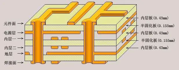
Tips: Multi-layer boards are often referred to in even numbers, such as 2, 4, 6, 8, 10~20~40~100 layers. Simply put, the number of copper layers corresponds to the number of layers of traces, which indicates the number of layers of the board. Currently, most multi-layer processes are made by laminating several double-sided copper boards, so the vast majority of multi-layer boards are even-numbered. For example, two double-sided boards laminated together form a 4-layer board, adding one double-sided board results in a 6-layer board, and so on.
Additionally, higher-level process technologies such as HDI, SLP, and Anylayer, despite their complexity and specificity, with many holes, fine lines, numerous processes, and high precision, still belong to the category of “hard boards” in simple classification, unless specifically listed otherwise.

2:By Material Properties

(Uh, the editor is not sure if this image can adequately represent soft and hard)
Circuit boards can be classified by material properties into flexible boards (FPC), rigid boards (PCB), and rigid-flex boards (FPCB).
As the name suggests, flexible boards are highly bendable, made from softer materials, and are used in electronic products that require stretching, bending, and three-dimensional assembly, such as cameras, camcorders, printers, smartphones, etc. The main substrates are PI, LCP, PPE, etc.;
Rigid boards, also known as hard boards, were originally made from paper-based materials, but now are commonly made from FR4, which is electronic-grade glass fiber woven into electronic cloth (similar to the principle of a loom), then wetted with resin and double-sided copper foil is applied. Their characteristics include high hardness, stability, and good insulation. Due to their material having significant hardness (mechanical strength), they not only serve to connect circuit traces but also act as a foundation for many small electronic components, thus earning the title of “mother of electronics”.
In the 5G era, to meet the demands of high frequency and speed, more materials are continuously being developed, with PTFE being a well-known example, which has a certain degree of flexibility compared to FR4, thus presenting greater processing challenges.
Of course, the above are just examples of different base materials to distinguish between flexible and rigid boards. In reality, both flexible and rigid boards have dozens of material classifications, and even if the main materials are similar, their fillers (powders that enhance hardness, etc.) vary, and proportions differ significantly. Each supplier has its own patented technology, which is not listed here.
Tips: For example, in smartphones, the mainboard and button board are rigid boards, carrying the majority of electronic components; early sliding or flip phones used flexible connectors, while most modern smartphones have three-dimensional packaging, requiring flexible connections for sensors, camera modules, batteries, antennas, etc. The latest foldable phones will also have a significant demand for flexible boards.
3:By Downstream Applications

This classification is often mentioned by marketing personnel in the circuit board market, as it directly relates to the customer attributes and the end applications of the circuit boards, hence referred to by application names.
Regardless of whether they are flexible or rigid boards, their end applications are numerous:
Mobile phone boards, charger boards;
Communication base station boards, antenna boards, power supply boards, server motherboards, computer mainboards, mouse boards, graphics card boards, memory stick boards;
Office equipment such as printer boards, copier boards;
Home appliances such as digital camera boards, radio boards, television mainboards, set-top box boards, washing machine/air conditioner/kitchen appliances/vacuum cleaner/refrigerator/audio-visual equipment boards, LED lamp boards;
Industrial control boards, instrument boards;
Automotive boards, charging pile boards, GPS navigation boards;
Medical instrument boards;
Aerospace, missile satellites, military weapons, and other applications.
4: By Subdivided Material Properties
According to the flame retardancy of copper-clad laminates (CCL), they can be classified into flame-retardant types (UL94-V0, UL94-V1) and non-flame-retardant types (UL94-HB). In recent years, with increasing attention to environmental issues, a new type of bromine-free CCL has emerged within the flame-retardant CCL category, which can be referred to as “green flame-retardant CCL”.
With the rapid development of electronic product technology, there are higher performance requirements for CCL. Therefore, from the performance classification of CCL, it can be divided into general performance CCL, low dielectric constant CCL, high heat resistance CCL (generally above 150°C for standard boards), low thermal expansion coefficient CCL (generally used in packaging substrates), and other types.
5:By PCB Surface Treatment Classification
This classification is more common in factories and among technical personnel, mainly referring to commonly used process flows. For example, PCB surface treatment classifications include leaded tin-spray boards (containing copper, tin, lead), lead-free tin-spray boards (mainly composed of copper, tin, with trace amounts of nickel, silver, gold), gold-plated boards (containing copper, nickel, gold), chemical gold boards (containing copper, nickel, gold), anti-oxidation or OSP boards (containing copper), gold finger boards (suitable for plug-in edge gold finger processes), chemical silver boards, selective gold boards, etc.
6:Types of Special Printed Boards
Currently, there are also metal core printed boards, carbon film printed boards, glass substrates, ceramic substrates, and other special printed boards on the market. These categories are distinguished by their special substrates.
Metal Core Printed Boards
Metal core printed boards replace epoxy glass cloth boards with a metal plate of equivalent thickness, and after special treatment, the conductive circuits on both sides of the metal plate are interconnected while being highly insulated from the metal part. The advantages of metal core printed boards include good heat dissipation and dimensional stability, as materials like aluminum and iron have shielding effects that can prevent mutual interference.
Metal core substrates, also known as heat dissipation substrates, primarily utilize the heat dissipation properties of metals. As electronic products become smaller and more integrated, the heat generated by their functions poses a significant challenge for rapid dissipation. Therefore, metal core heat dissipation substrates have become a major category in applications involving high current and high efficiency products.
Metal cores mainly include copper-based, iron-based, and aluminum-based.
Carbon Film Printed Boards
Carbon film printed boards are created by printing a layer of carbon film (conductive ink) on an insulator to form contacts or jumpers (with resistance values meeting specified requirements).
Carbon film, as the name suggests, is a thin film formed by carbon ink particles adhered to an insulating substrate.
The main feature is a simple screen printing process, where the conductive pattern is made using conductive ink instead of the common copper layer for traces; it can also add one or two layers of conductive patterns on single-sided printed boards to achieve high-density wiring. The conductive patterns not only interconnect but also serve as resistors, button switch contacts, and electromagnetic shielding layers.
Its process characteristics include simple production, low cost, short cycle, good wear resistance, and conductivity, allowing single-sided boards to achieve high density, miniaturization, and lightweight, suitable for products like televisions, telephones, game consoles, calculators, and electronic keyboards.
Glass Circuit Boards
Calculator, mobile phone, telephone, and many other electrical devices’ LCD screens are made from glass circuit boards! The circuits connecting the LCD and the LCD itself are made on the glass surface, but cannot be connected to external circuits using soldering methods, only through elastic soft contacts for mechanical connection.
A type of transparent glass-based circuit board, where the glass substrate and conductive lines are in a fused relationship, tightly connected, and the surface of the glass substrate is flush with the surface of the conductive lines, resulting in a smooth surface for the high-conductivity transparent glass-based circuit board, making the conductive lines less prone to damage and providing strong conductivity.
Evenly distributed throughout the glass substrate are conductive holes that penetrate the glass substrate, with hollow copper tubes set within the conductive holes, the ends of which are flush with the surface of the glass substrate; both the upper and lower surfaces of the glass substrate have conductive lines fused with the glass substrate, and the two conductive lines are connected through the hollow copper tubes. The conductive lines can be made of graphene or a conductive layer composed of a surface graphene layer and a bottom layer fused with the glass substrate, with the contact surfaces between the graphene layer and the metal layer being mutually fused. The glass substrate is made of tempered glass.
Ceramic Circuit Boards
These are made using thermally conductive ceramic powder and organic binders, producing thermally conductive organic ceramic circuit boards with thermal conductivity coefficients of 9-20W/m.k at temperatures below 250°C.
As electronic technology gradually deepens in various application fields, the high integration of circuit boards has become an inevitable trend. Highly integrated packaging modules require good heat dissipation systems, while traditional FR-4 and CEM-3 circuit boards have disadvantages in thermal conductivity (TC), which has become a bottleneck restricting the development of electronic technology. In recent years, the rapidly developing LED industry has also raised higher requirements for the TC indicators of their supporting circuit boards. In the high-power LED lighting field, materials with good heat dissipation properties, such as metals and ceramics, are often used to manufacture circuit substrates, with high thermal conductivity aluminum substrates generally having thermal conductivity coefficients of 1-4W/M.K, while ceramic substrates can reach around 220W/M.K depending on their manufacturing methods and material formulations.
Main Advantages
Unlike traditional FR-4 (wave fiber), ceramic materials have excellent high-frequency performance and electrical properties, as well as high thermal conductivity, chemical stability, and thermal stability that organic substrates do not possess, making them ideal packaging materials for the next generation of large-scale integrated circuits and power electronic modules.
1. Higher thermal conductivity
2. Better matching thermal expansion coefficients
3. Stronger, lower-resistance metal film layers on aluminum oxide ceramic circuit boards
4. Good solderability of the substrate, high operating temperature
5. Good insulation
6. Low high-frequency loss
7. Capable of high-density assembly
8. Free of organic components, resistant to cosmic rays, high reliability in aerospace applications, and long service life
9. Copper layers free of oxidation can be used for long periods in reducing atmospheres
Common Processes
The traditional preparation methods for ceramic substrates can be divided into four main categories: HTCC, LTCC, DBC, and DPC.
HTCC (High-Temperature Co-Firing) requires temperatures above 1300°C, but the choice of electrodes significantly affects the cost of production, making it quite expensive;
LTCC (Low-Temperature Co-Firing) requires about 850°C for sintering, but the precision of the produced circuits is relatively poor, and the thermal conductivity of the finished product is lower;
DBC (Direct Bonding Copper) requires the formation of an alloy between copper foil and ceramic, with strict control of the sintering temperature between 1065-1085°C. Due to the requirements for copper foil thickness, generally not less than 150-300 microns, this limits the wire width-to-depth ratio of such ceramic circuit boards.
DPC (Direct Print Circuit) involves vacuum coating, wet coating, exposure, development, etching, and other process steps, making its products relatively expensive. Additionally, DPC ceramic boards require laser cutting for shape processing, as traditional drilling and punching machines cannot achieve precise processing, thus requiring finer bonding strength and line width spacing.

Some Screenshots from Electronic Books
【Complete Set of Hardware Learning Materials Collection】