From smartphones to AI servers, from new energy vehicles to satellite communications, the efficient operation of every electronic device relies on an “invisible cornerstone”—the PCB (Printed Circuit Board).
As the “nerve center” of electronic components, it carries the core functions of signal transmission and power distribution, spanning the entire electronics industry chain. Its technological iteration and industrial pattern directly influence the pace of global technological development.
Today, with the explosive growth of AI computing power, the acceleration of electric and intelligent vehicles, and the deepening application of 5G, the PCB industry is entering a high-growth cycle worth trillions. China has captured 56% of the global production capacity, becoming the industry leader.
This article will comprehensively explain the development logic and future opportunities of this “mother of the electronics industry” from five dimensions: definition, market, applications, industry chain, and company overview.
1. What is PCB? The “Nerve Center” of Electronic Devices
PCB (Printed Circuit Board) is the core support and electrical connection carrier of electronic components, known as the “mother of electronic systems.”
It achieves signal transmission and power distribution for components such as chips, resistors, and capacitors through a pre-designed circuit layout, making it an indispensable basic component of all electronic devices.
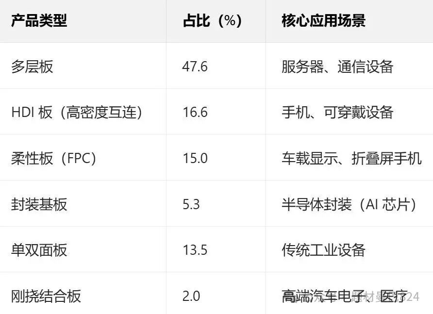
In terms of types, PCBs can be divided into rigid boards, flexible boards (FPC), rigid-flex boards, high-density interconnect boards (HDI), and packaging substrates, among other subcategories.
As electronic devices evolve towards miniaturization and high performance, PCBs are iterating towards high density, high frequency, and high reliability, with line widths/spacing compressed to below 30μm. Some high-end products even reach levels of 20/35μm, equivalent to one-third the diameter of a human hair.
2. Market Prospects for PCBs: A Trillion-Dollar High-Growth Cycle
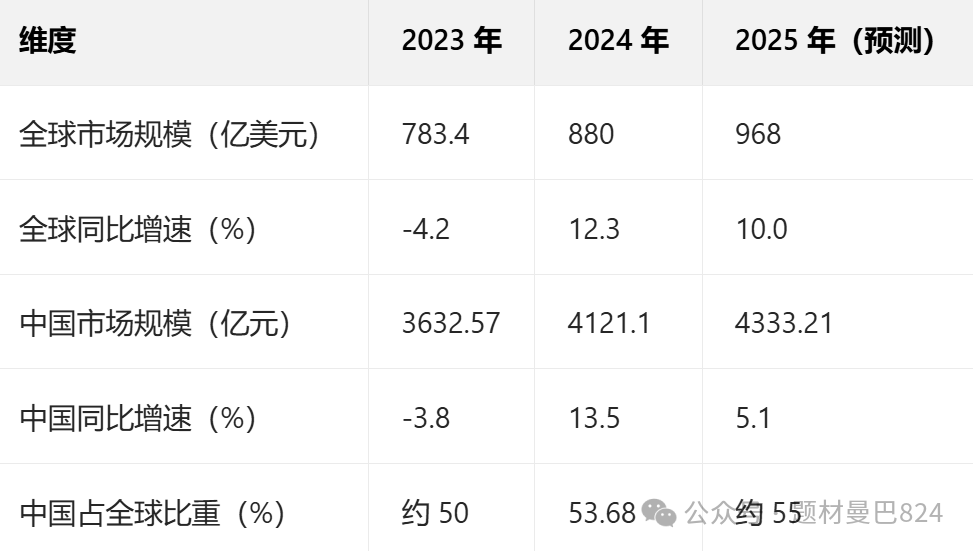
The global PCB market has emerged from an adjustment period and entered a stable growth channel. By 2024, the total global PCB output value is expected to reach $73.565 billion, a year-on-year increase of 5.8%. It is projected to exceed $96.8 billion in 2025 and reach $94.661 billion by 2029, with a compound annual growth rate (CAGR) of 5.2% from 2024 to 2029.
China has become the core engine of the global PCB industry, with an output value of $41.213 billion in 2024, accounting for 56% of the global share, and is expected to increase to $43.734 billion in 2025, further enhancing its share.
In the high-end PCB sector (multi-layer boards with more than 8 layers, HDI, packaging substrates, etc.), China’s production capacity has surged to over 95%, completely dominating the global high-end supply.
The core drivers of market growth come from three major tracks: explosive growth in demand for AI servers, increasing penetration of new energy vehicles driving up the value of automotive PCBs, and emerging technologies such as 5G, IoT, and satellite communications continuously opening up application spaces.
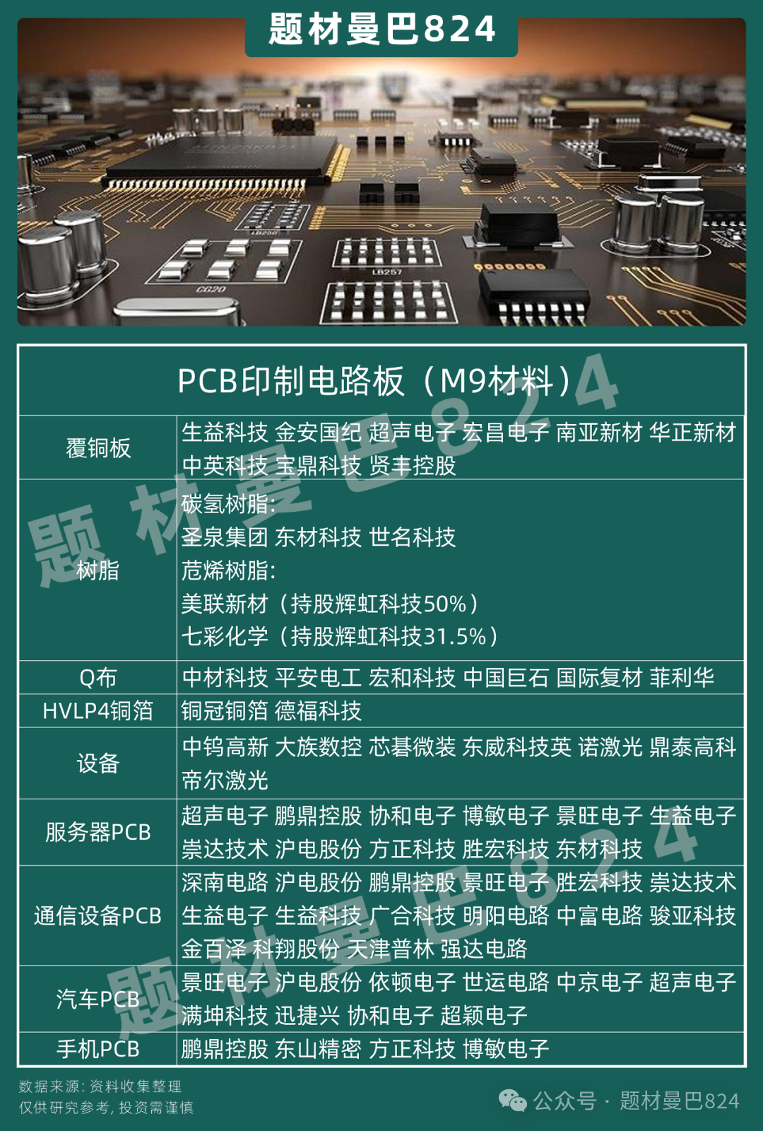
NVIDIA expects that the PCBs for the cpx and midplace in the Rubin series, which will be released in the second half of next year, will use M9 CCL, and they are evaluating whether compute and switchtray will use M9; the Rubin ultra for 2027 will definitely use orthogonal backplanes instead of copper boards, effectively upgrading the PCB industry chain towards high-end and precision.
3. Differences Between NVIDIA M9 and Ordinary PCB Materials
NVIDIA M9, designed specifically for AI computing power, has generational differences in materials, processes, and performance compared to ordinary PCBs. The core differences are as follows:
1. Disruptive Upgrade of Material System
M9 uses a hydrocarbon (PCH)/exciplex (EX) resin system, with a dielectric loss (Df) as low as 0.0005-0.0006, only 1/40 of the traditional FR-4 resin (Df≈0.02). The reinforcing material is replaced with quartz fabric (Q fabric) instead of fiberglass, and the thermal expansion coefficient (CTE) is reduced to 5ppm/°C, maintaining a warpage rate within 0.5% at high temperatures of 150°C.
Paired with HVLP4 ultra-low profile copper foil (surface roughness Rz<0.2μm), signal reflection loss is reduced by 60%, supporting ultra-high-speed transmission of 224Gbps. Additionally, the inclusion of 40% spherical silica filler doubles the delamination resistance, adapting to complex stress environments.
2. Extreme Breakthrough in Manufacturing Process
M9 supports 78-layer orthogonal backplane design, achieving a global bandwidth of 12.8Tbps through three-dimensional integration, with inter-layer alignment accuracy of ±5μm. Its processing requires nano-diamond coated drill bits (with a lifespan of only 100-200 holes) and ultra-fast laser drilling equipment (accuracy ±8μm), with drilling costs 2-3 times that of ordinary PCBs. Surface treatment uses chemical nickel gold (ENIG) or organic solder mask (OSP), certified by AEC-Q100 automotive standards, and can operate stably in environments from -40°C to 85°C.
3. Generational Performance and Application Gap
In terms of signal integrity, M9 has a transmission loss of only 0.18dB/cm at a frequency of 10GHz, which is 40% lower than M8 materials, supporting ultra-high-speed interfaces such as 800G switches and 1.6T optical modules. Its heat dissipation capability significantly outperforms ordinary PCBs, with a thermal conductivity of 1.2W/m・K, capable of handling chip power densities of 200W/cm² when combined with microchannel liquid cooling.
Application fields are concentrated in NVIDIA Rubin architecture AI servers (such as 576-card clusters), roadside units (RSUs) for autonomous driving, etc., with a single machine value of up to $200,000, while ordinary PCBs are mostly used in consumer electronics, with a single board cost of less than $100.
4. Industry Chain and Cost Structure
M9 copper-clad laminates are led by Panasonic and Shengyi Technology, while Q fabric relies on Fihua and Taiko Electric, and HVLP4 copper foil is mass-produced by Cuprum. Material costs are three times that of traditional solutions, and the 78-layer orthogonal backplane increases the single board value by 300%, accounting for 37%-40% of the total cost of AI servers. In contrast, ordinary PCB material suppliers are dispersed, with cost accounting for only 10%-15%.
NVIDIA M9, through innovations in hydrocarbon resin, quartz fabric, and other materials, combined with ultra-high layer design and precision manufacturing processes, has broken through the performance bottleneck of ordinary PCBs, becoming the core material supporting the explosion of AI computing power.
4. Applications of PCBs Across Industries: Penetrating the Entire Electronics Industry Chain
1. Communication Equipment: Core Support in the 5G Era
Communication equipment is the largest application field for PCBs, accounting for 28.4%, covering 5G base stations, routers, optical modules, etc. The Massive MIMO technology of 5G base stations requires PCBs to have extremely low dielectric loss (Df≤0.002), significantly increasing the number of integrated channels per base station PCB, driving demand for high-frequency and high-speed PCBs. By 2025, the combined capital expenditure of the four major cloud service providers is expected to exceed $330 billion, further boosting the growth of communication-related PCBs.
2. Automotive Electronics: Incremental Engine for Electrification and Intelligence
The popularity of new energy vehicles has completely activated the automotive PCB market. The value of PCBs in traditional fuel vehicles is only $60-100 per vehicle, while electric intelligent vehicles have increased to over $500, and L4 autonomous vehicles exceed $2,000.
By 2025, the penetration rate of new energy vehicles in China is expected to exceed 50%, with L3 autonomous driving penetration reaching 25%. The three electric systems, ADAS, and cockpit domain control will become core demand scenarios, driving the automotive PCB market scale to exceed 20 billion yuan.
3. AI Servers: The “Growth Engine” of High-End PCBs
The exponential growth in demand for AI computing power has made AI servers the core driving force for the high-endization of PCBs. In 2023, the global market size for AI server PCBs is close to $800 million, and it is expected to reach $3.17 billion by 2028.
The value of a single AI inference server PCB is $1,200-1,500, five times the premium over ordinary servers, with a significant supply-demand gap for high multi-layer boards and high-end HDI products.
4. Consumer Electronics and Emerging Fields
Although the consumer electronics field has entered a mature stage, innovative terminals such as AI phones, AR/VR devices, and smart home products are driving an increase in demand for flexible circuit boards (FPC), with AI phone FPC usage increasing by 30% compared to traditional phones.
Additionally, there is strong demand for special PCBs in aerospace, medical devices, and low-orbit satellites, with satellite PCBs needing to withstand extreme environments from -270°C to +120°C, significantly higher in technical added value than ordinary products.
5. Upstream and Downstream Analysis of PCBs: China-Dominated Industry Chain Ecology
1. Upstream: Raw Materials and Equipment, High-End Materials Await Breakthrough
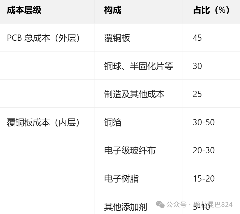
The upstream core links include raw materials and production equipment. Among raw materials, copper-clad laminates account for over 35% of PCB costs. Domestic companies such as Shengyi Technology and Kingboard Chemical have entered the global first tier, with a self-sufficiency rate of over 80% for high-frequency and high-speed copper-clad laminates, breaking the foreign monopoly; the localization rate of key materials such as copper foil, resin, and fiberglass cloth continues to rise.
In the equipment sector, the localization rate of drilling, plating, and laminating equipment has reached over 56.5%, with plating equipment holding a global market share of 84.8%. However, high-end equipment such as exposure lithography machines still relies on imports, with some high-end photoresists having an import dependency of over 50%, becoming a key bottleneck for industry chain upgrades.
2. Midstream: Manufacturing Links, China Holds Absolute Advantage
The midstream is the core link of PCB design and manufacturing. China has formed three major industrial clusters in the Pearl River Delta, Yangtze River Delta, and Bohai Rim, with Guangdong Province accounting for over 40% of the national PCB output.
Seven of the top ten PCB companies globally are from China, with leading companies such as Shenzhen Sunway, Hubei Electric, and Unimicron Technology leading in AI server PCBs, packaging substrates, and flexible boards, with high-end product yields exceeding 95%.
By 2025, the output value of PCBs in China (including Hong Kong and Taiwan) is expected to account for 75.2% of the global share, with production capacity in high-end fields such as multi-layer boards with more than 8 layers reaching over 95%, achieving a leap from “scale first” to “technology leading”.
3. Downstream: End Applications, Diversified Demand Drives Growth
The downstream covers multiple fields including communication equipment, automotive electronics, consumer electronics, AI servers, and aerospace. Major terminal giants such as Huawei, ZTE, Tesla, Microsoft, and NVIDIA have become core purchasers of PCBs, with leading PCB companies having an order visibility of 8-10 months overseas. Among them, the server/storage and aerospace sectors are growing the fastest, expected to reach 33.1% and 7.4% respectively by 2024, significantly higher than the industry average.
6. Conclusion: New Opportunities in the Industry Under High-End and Globalization
As the “invisible cornerstone” of the electronics industry, the development level of PCBs directly reflects a country’s comprehensive competitiveness in the electronic information industry. Currently, the industry is in a golden development period of “demand explosion + technological breakthroughs + capacity restructuring,” with three major trends—AI computing power, automotive electrification, and deepening 5G—forming the core growth engines.
The Chinese PCB industry has formed a full industry chain advantage, leading globally in production capacity, technological iteration, and cost control, but some links in high-end materials and core equipment still need breakthroughs. In the future, the PCB industry will develop towards high-end (packaging substrates, high-frequency and high-speed boards), green (halogen-free materials, waste liquid recycling), and globalization (“China + N” capacity layout).
For enterprises, binding to high-growth tracks such as AI servers and smart vehicles, increasing core technology R&D, and laying out global production capacity will be key to seizing industry dividends. With the rise of emerging fields such as 6G and brain-computer interfaces, the application boundaries of PCBs will continue to expand, and the long-term value of the trillion-dollar market is worth looking forward to, with a focus on the application of M9.