
For those studying electronics, setting up test points on a circuit board is a natural practice.
How many people have not heard of test points? And how many know about test points but do not understand their purpose?The primary purpose of setting up test points is to test whether the components on the circuit board meet specifications and solderability. For example, if you want to check if a resistor on a circuit board is functioning correctly, the simplest method is to use a multimeter to measure its ends.However, in mass production factories, it is impractical to use a multimeter to slowly measure every resistor, capacitor, inductor, or even the IC circuits on each board. This led to the emergence of ICT (In-Circuit Test) automated testing machines.These machines use multiple probes (commonly referred to as “Bed-Of-Nails” fixtures) to simultaneously contact all the components and circuits that need to be measured on the board. They then sequentially and parallelly measure the characteristics of these electronic components through programmed control.Typically, testing all components on a standard board can be completed in about 1-2 minutes, depending on the number of components on the circuit board; the more components, the longer the time required.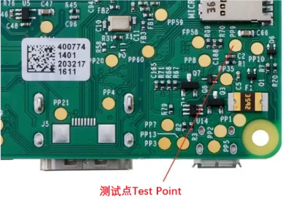 However, if these probes directly contact the electronic components or their solder joints on the board, it is very likely to damage some electronic components, which would be counterproductive.Thus, clever engineers invented “test points,” which are small circular pads added at both ends of the components, free of solder mask, allowing the test probes to contact these pads instead of directly touching the components being measured.In the early days of circuit boards, when traditional through-hole components (DIP) were prevalent, it was common to use the component’s solder pins as test points because the solder pins of traditional components were robust enough to withstand probe contact. However, this often led to misjudgments due to poor probe contact.After wave soldering or SMT soldering, a thin film of solder paste flux residue usually forms on the surface of the solder, which has very high impedance and often causes poor probe contact.As a result, it was common to see test operators on the production line using air guns to blow air onto the boards or using alcohol to wipe the areas that needed testing.In fact, test points that have undergone wave soldering can also experience poor probe contact issues. However, after the rise of SMT, the incidence of testing misjudgments has significantly improved, and the application of test points has been greatly enhanced.Because SMT components are usually very fragile and cannot withstand the direct contact pressure of test probes, using test points allows probes to avoid direct contact with the components and their solder joints, protecting the components from damage and indirectly greatly improving the reliability of testing, as the incidence of misjudgments has decreased.However, with the advancement of technology, the size of circuit boards has become smaller and smaller. Fitting so many electronic components onto a small circuit board has become challenging, leading to frequent discussions about the space occupied by test points between design and manufacturing teams.Test points are typically circular in shape because probes are also circular, making them easier to produce and allowing adjacent probes to be placed closer together, thereby increasing the density of the probe bed.Using a probe bed for circuit testing has some inherent mechanical limitations, such as the minimum diameter of the probes having a certain limit; probes with too small a diameter are prone to breakage and damage.The spacing between probes also has certain limitations because each probe must exit from a hole, and each probe’s rear end must be soldered to a flat cable.If the adjacent holes are too small, there will be issues with short circuits between probes, and interference from flat cables is also a significant problem.Some high components cannot have probes placed next to them; if the probes are too close to high components, there is a risk of collision causing damage. Additionally, because the components are taller, holes must be opened in the test fixture’s probe bed to avoid them, which indirectly leads to the inability to place probes, making it increasingly difficult to accommodate all component test points on the circuit board.As the boards become smaller, the number of test points is frequently discussed. Some methods to reduce test points have emerged, such as Net test, Test Jet, Boundary Scan, and JTAG.There are also other testing methods attempting to replace traditional probe bed testing, such as AOI and X-Ray, but currently, none of these tests seem to be able to 100% replace ICT.Regarding the probe placement capability of ICT, it is advisable to consult the fixture manufacturers involved, specifically about the minimum diameter of test points and the minimum distance between adjacent test points. Typically, there will be a desired minimum value and a minimum value that can be achieved, but large-scale manufacturers will require that the distance between the minimum test points does not exceed a certain amount; otherwise, the fixtures may be easily damaged.


Some screenshots from electronic books

【Complete Set of Hardware Learning Materials Collection】