In the previous popular science comic series,
we got to know the “photo-taking hero” ISP,
and experienced the intelligent NPU.
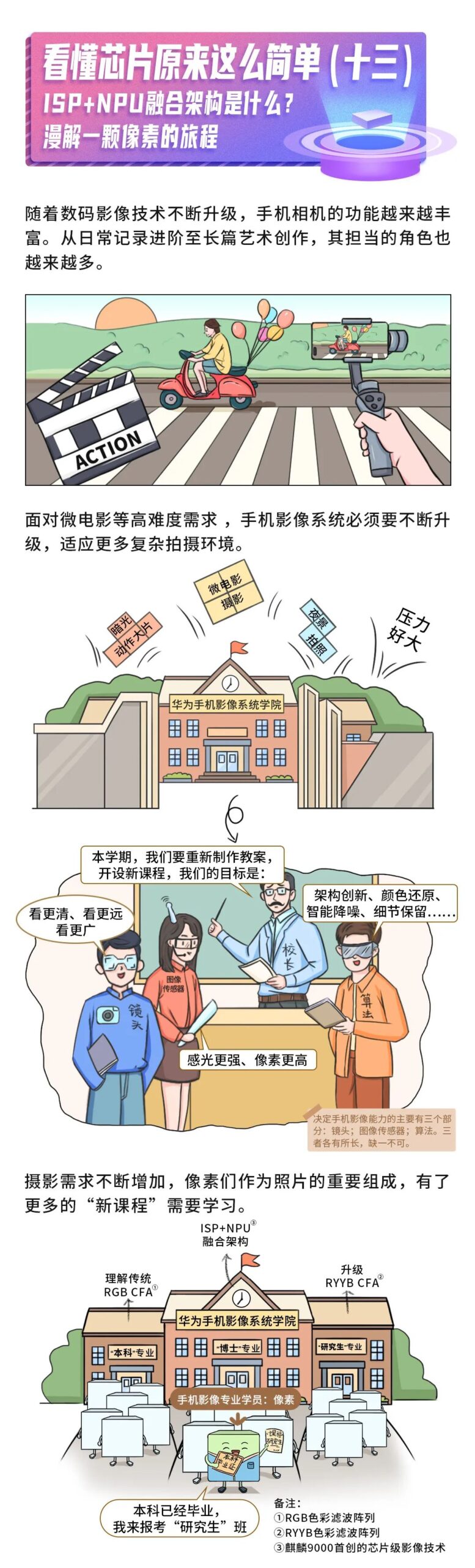
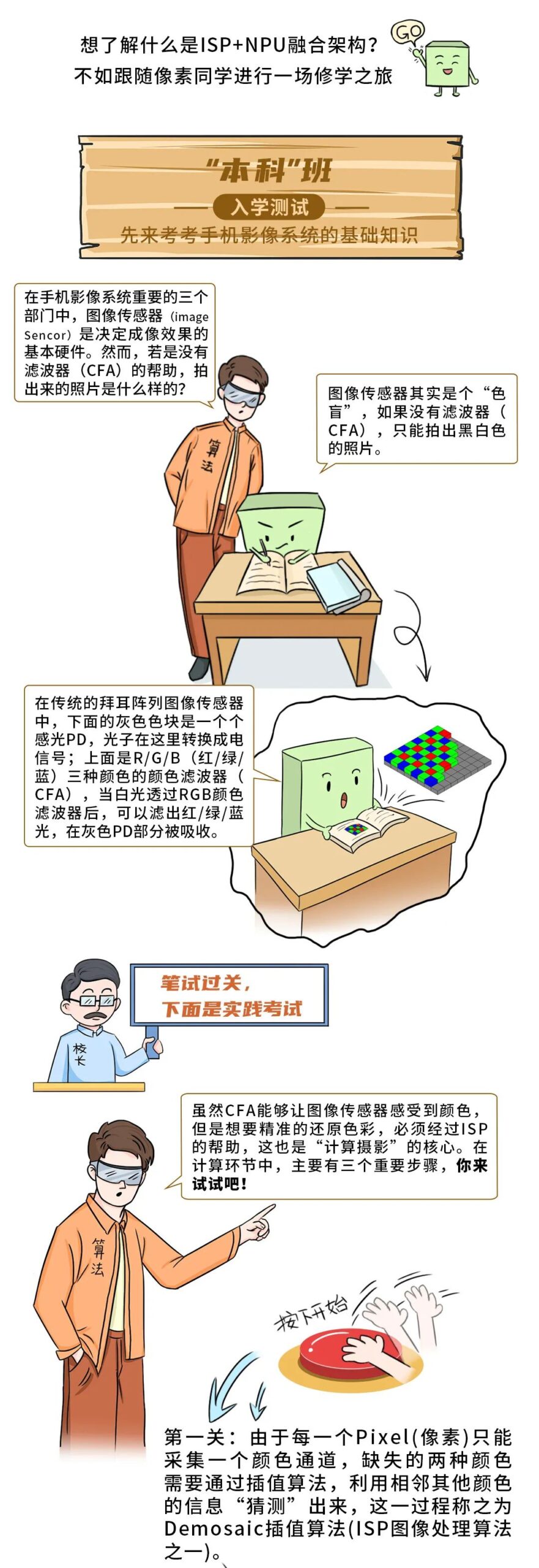
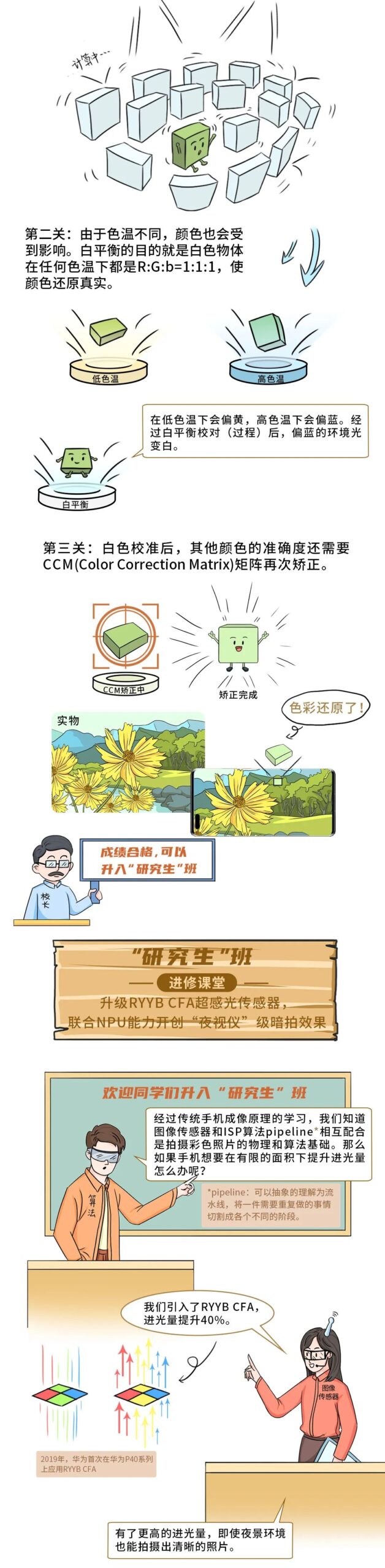
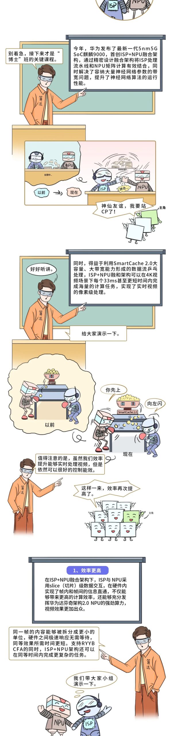
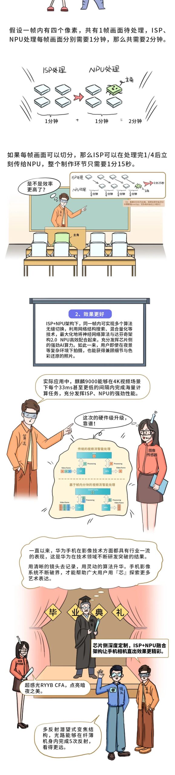
So what is the ISP+NPU fusion architecture?
In this issue, we will follow “a pixel” on its journey,
delving into the “core” world,
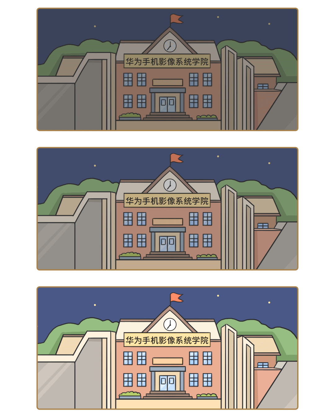
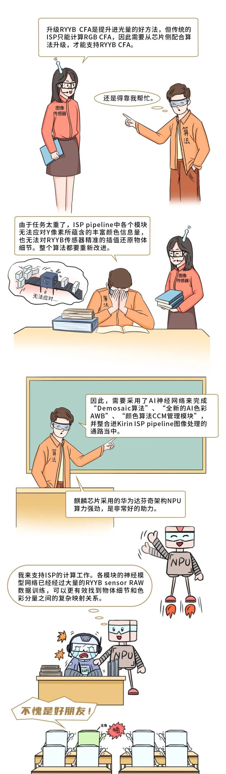
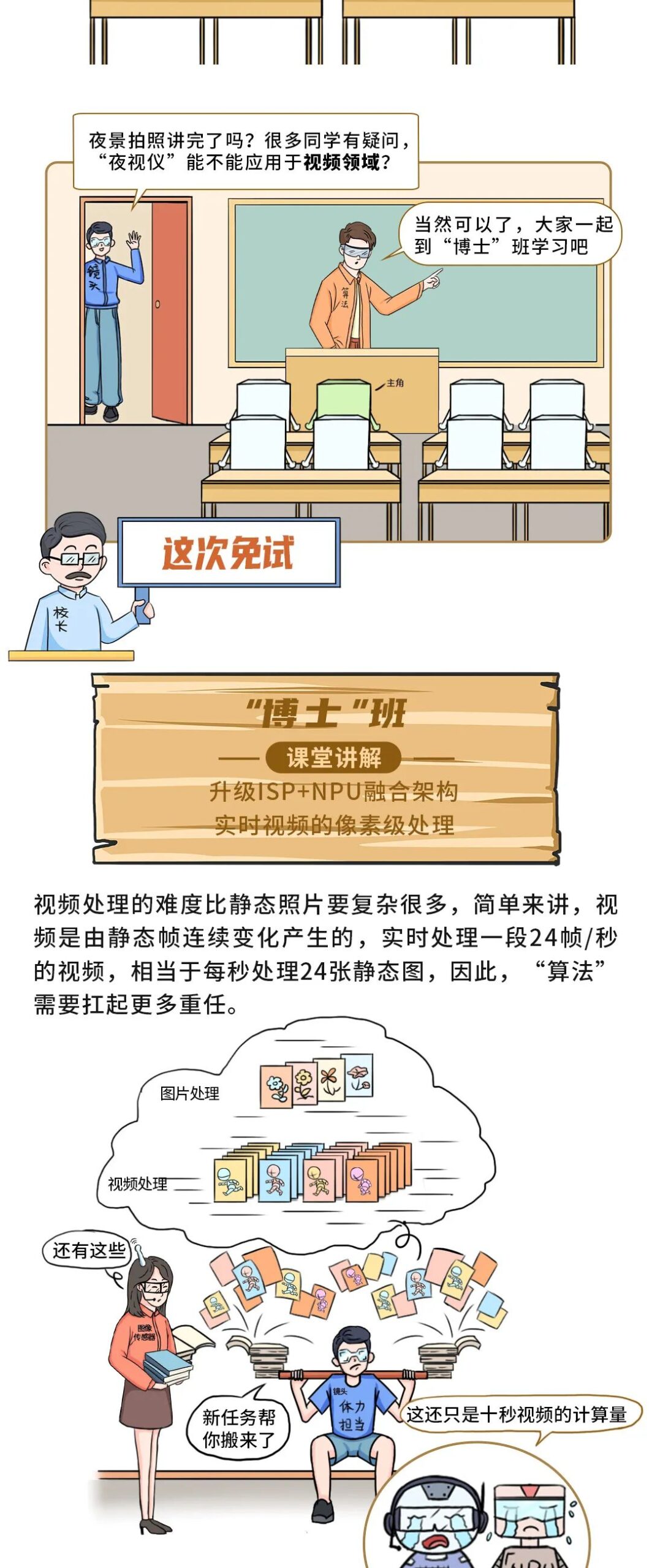
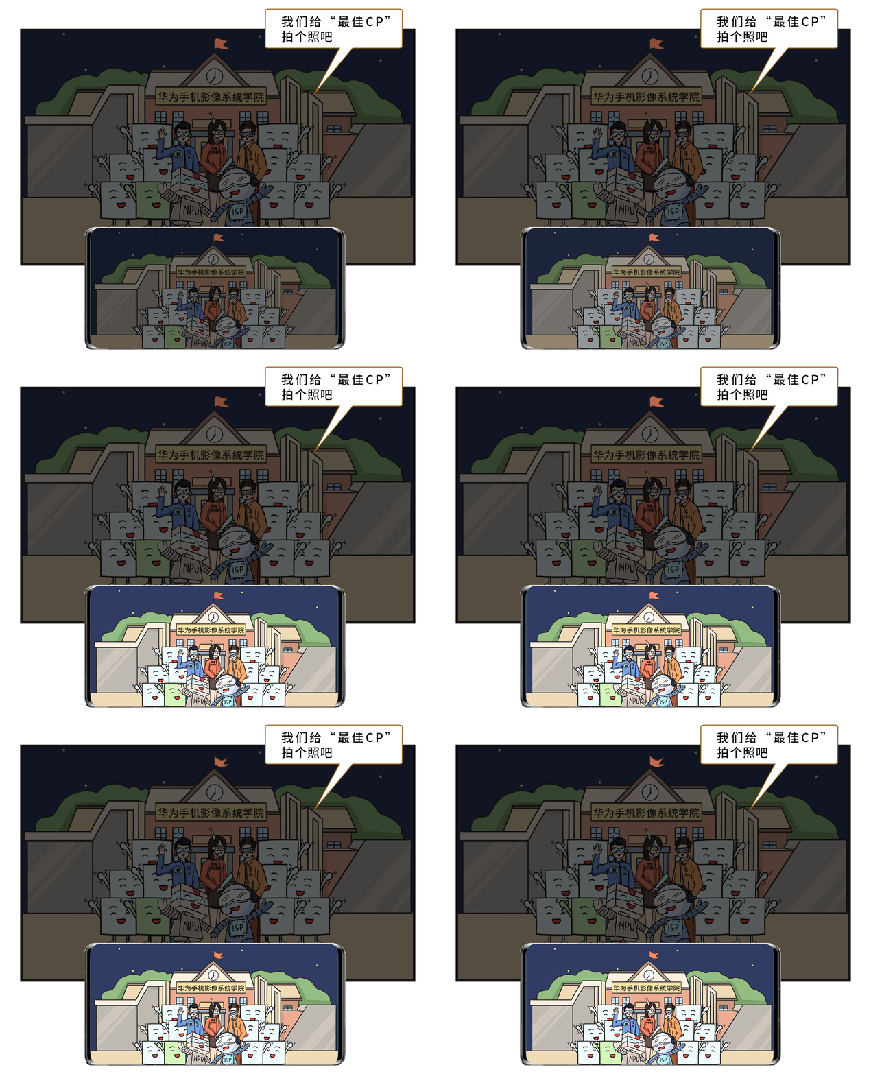
revealing the entire process of how the Kirin 9000 conquers night photography.
 Previous Issues:1. What are integrated circuits/processes/CPU/GPU?2. Why is AI so smart? Huawei’s self-developed architecture NPU!3. Ding~ It’s class time, let’s understand 5G chips in seconds!4. When taking photos with a phone, do you look at the lens or the pixels? Look at ISP!5. Complete explanation of Huawei Wi-Fi6+!6. Essential for calls – RF!7. Where does all the data in a phone reside? memory!8. How does the chip protect digital copyright?9. The “fast calculator” of digital signals – DSP!10. Huawei’s open capability upgrade, introducing 2 new members!11. How do Bluetooth, Wi-Fi, and GNSS cooperate?12. How is a chip designed?Test yourself (5 points) What is CFA?(Hurry to the comment section to answer!)Huawei Kirin original content Huawei Kirin original content Huawei Kirin original contentcontentScan the QR code to follow Huawei Kirin
 Support Kirin~ Like
  Looking