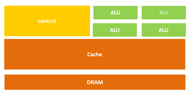
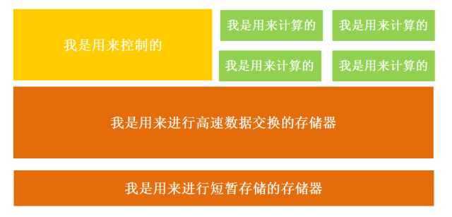
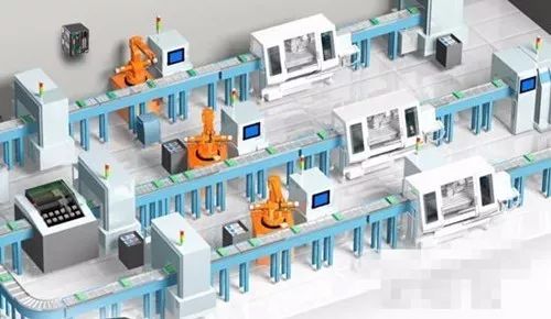
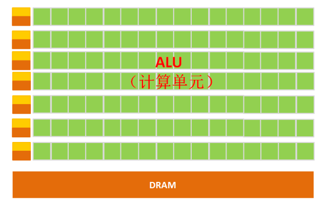
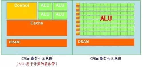
The GPU uses many simple computational units to complete a large number of computational tasks, purely a human wave tactic.
This strategy is based on one premise: that the work of elementary school students A and B is independent of each other.
However, one point needs to be emphasized: although the GPU was born for image processing, we can see from the previous introduction that it does not have components specifically designed for image services; it is merely an optimization and adjustment of the CPU’s structure, so now GPUs can not only excel in image processing but are also used in scientific computing, cryptography, numerical analysis, massive data processing (sorting, Map-Reduce, etc.), financial analysis, and other fields that require large-scale parallel computing.
Therefore, the GPU can also be considered a relatively general-purpose chip.
According to the above, both the CPU and GPU are relatively general-purpose chips, but there’s an old saying:The efficiency of a universal tool is always inferior to that of a specialized tool.
As people’s computing needs become more specialized, they hope for chips that better fit their professional requirements, leading to the concept of ASIC (Application-Specific Integrated Circuit).
ASIC refers to special specification integrated circuits customized based on product requirements, designed and manufactured according to the needs of specific users and specific electronic systems. Of course, this concept doesn’t need to be remembered; in simple terms, it means customized chips.
Because ASICs are very “specialized” and only do one thing, they can perform better than chips like CPUs and GPUs that can do many things, achieving higher processing speeds and lower energy consumption. However, correspondingly, the production cost of ASICs is also very high.
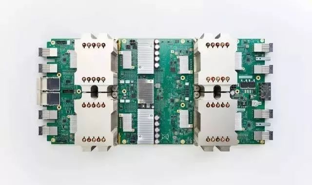
And TPU (Tensor Processing Unit) is a chip developed by Google specifically to accelerate deep neural network computation capabilities, which is actually also an ASIC.
Figure: Google’s Second Generation TPU
Generally, it is difficult for companies to bear the cost and risk of developing specialized ASIC chips for deep learning, but who is Google? They don’t lack money, right?
Just kidding. The more important reason is that many services provided by Google, including Google Image Search, Google Photos, Google Cloud Vision API, Google Translate, etc., require deep neural networks. Based on Google’s huge scale, developing a dedicated chip has begun to have the possibility of large-scale application (spreading the R&D costs over a large volume).
Thus, it is logical for TPU to take the stage in history.
Many machine learning and image processing algorithms originally ran on GPUs and FPGAs (field-programmable gate arrays), but these two types of chips are still general-purpose chips, so in terms of performance and power consumption, they cannot be more closely adapted to machine learning algorithms. Google has always believed that great software will shine even brighter with the help of great hardware, so Google thought, can we create a dedicated machine learning algorithm chip? Thus, the TPU was born.
It is said that TPUs can provide a 15-30 times performance improvement and a 30-80 times efficiency improvement (performance/watt) compared to CPUs and GPUs of the same period. The first generation TPU could only perform inference, relying on Google Cloud to collect data in real-time and produce results, while the training process required additional resources; while the second generation TPU can be used for both training neural networks and inference.
At this point, you may ask, why is the TPU so powerful in terms of performance?
Well, Google has written several papers and blog posts explaining this reason, so I’ll just throw out a hint here.
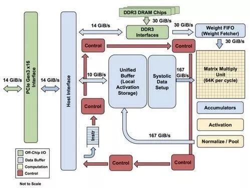
Figure: TPU Module Block Diagram
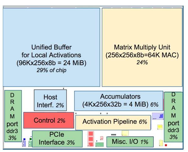
Figure: TPU Chip Layout Diagram
As shown in the figure, the TPU has up to 24MB of local memory, 6MB of accumulator memory, and memory used to interface with the main control processor, occupying 37% of the chip area (the blue part in the figure).
This indicates that Google fully realizes that external memory access is the culprit for the low energy efficiency of GPUs, thus sparing no expense in putting huge memory on the chip. In contrast, NVIDIA’s K80 at the same time only has 8MB of on-chip memory, requiring constant access to external DRAM.
Additionally, the TPU’s high performance also comes from its tolerance for low computation precision. Research results show that the accuracy loss from low precision computation is very small, but it can bring huge convenience in hardware implementation, including lower power consumption, faster speed, smaller area of computational units on the chip, and lower memory bandwidth requirements… The TPU uses 8-bit low precision computation.
For more information, you can refer to Google’s papers.
So far, TPUs have already accomplished a lot, such as the machine learning artificial intelligence system RankBrain, which helps Google process search results and provide users with more relevant search results; also Street View, which improves the accuracy of maps and navigation; of course, there’s also the computer program AlphaGo for playing Go!
At this point, I believe everyone has a certain understanding of these so-called “XPUs”. Let’s continue.
The so-called NPU (Neural Network Processing Unit) is a neural network processor. As the name implies, this device aims to simulate human neurons and synaptic structures using circuits!
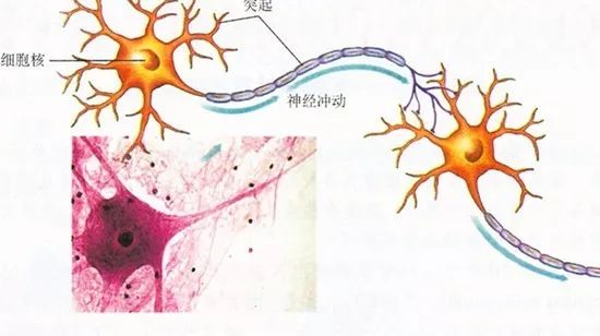
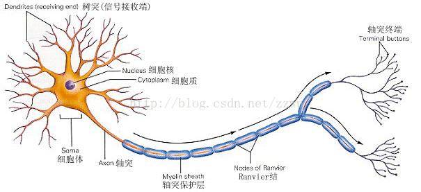
How to imitate? Then we need to take a look at the human neural structure—biological neural networks consist of several interconnected artificial neuron nodes, with neurons connected pairwise through synapses, and synapses record the connections between neurons.
Do you remember high school biology, comrades?
If we want to use circuits to mimic human neurons, we need to abstract each neuron as an activation function, the input of which is determined by the outputs of the neurons it is connected to and the synapses connecting the neurons.
To express specific knowledge, users typically need to adjust the values of synapses, the topology of the network, etc. (through certain specific algorithms). This process is called “learning”.
After learning, the artificial neural network can solve specific problems using the acquired knowledge.
At this point, I wonder if anyone has noticed a problem—originally, since the basic operations of deep learning involve processing neurons and synapses, while traditional processor instruction sets (including x86 and ARM, etc.) have been developed for general computing, their basic operations involve arithmetic operations (addition, subtraction, multiplication, division) and logical operations (AND, OR, NOT), often requiring hundreds or even thousands of instructions to complete the processing of a single neuron, resulting in low efficiency for deep learning processing.
This is where we must take a different approach—break through the classic Von Neumann architecture!
In neural networks, storage and processing are integrated, both represented through synaptic weights. In contrast, in the Von Neumann architecture, storage and processing are separated, implemented by memory and processors respectively, leading to a huge difference. When using existing classical computers based on the Von Neumann architecture (like x86 processors and NVIDIA GPUs) to run neural network applications, they inevitably face the constraints of the separated structure between storage and processing, thus affecting efficiency. This is one of the reasons why specialized chips for artificial intelligence have a certain inherent advantage over traditional chips.
Typical representatives of NPUs include China’s Cambricon chips and IBM’s TrueNorth. Taking China’s Cambricon as an example, the DianNao instruction directly faces the processing of large-scale neurons and synapses, completing the processing of a group of neurons with a single instruction, and providing a series of specialized support for the transmission of neuron and synapse data on the chip.
To put it in numbers, compared to CPUs and GPUs, NPUs can have a performance or energy efficiency ratio difference of over a hundred times—taking the DianNao paper jointly published by the Cambricon team and Inria as an example—DianNao is a single-core processor with a frequency of 0.98GHz, achieving a peak performance of 452 billion basic neural network operations per second, with a power consumption of 0.485W at a 65nm process, occupying an area of 3.02 square millimeters.
The Kirin 970 chip used in the Mate 10 mentioned at the beginning of the article integrates Cambricon’s NPU, enabling it to achieve so-called photo optimization functions and ensuring that your phone does not lag even after prolonged use (of course, you’ll only know if it lives up to the hype after actually using it).
PS: Although Zhongxing Microelectronics’ “Starlight Intelligent No. 1” is publicly claimed to be an NPU, it is actually just a DSP that only supports forward computation of networks and cannot support neural network training.
Based on all the knowledge above, it will be easier for us to understand BPU and DPU.
BPU (Brain Processing Unit) is an embedded artificial intelligence processor architecture proposed by Horizon Robotics. The first generation is the Gaussian architecture, the second generation is the Bernoulli architecture, and the third generation is the Bayesian architecture. Currently, Horizon has designed the first generation Gaussian architecture and jointly launched the ADAS system (Advanced Driver Assistance System) with Intel at the 2017 CES exhibition.
DPU (Deep Learning Processing Unit) was first proposed by Deep Insight Technology, based on the reconfigurable characteristics of Xilinx FPGA chips, designing dedicated deep learning processing units (which can be designed based on existing logic units, parallel efficient multipliers, and logic circuits, belonging to the IP category), and abstracting customized instruction sets and compilers (rather than using OpenCL), thus achieving rapid development and product iteration. In fact, the DPU proposed by Deep Insight belongs to semi-custom FPGA.
Did you think it was over here?
No, it is said that every 18 days, a new XPU will emerge in the integrated circuit field until all 26 letters have been used up.
This is humorously referred to as the XPU version of Moore’s Law in the AI era.
According to incomplete statistics, the following have already been used:
APU — Accelerated Processing Unit, AMD’s accelerated graphics processing chip product.
BPU — Brain Processing Unit, an embedded processor architecture led by Horizon.
CPU — Central Processing Unit, currently the mainstream product of PC core.
DPU — Deep Learning Processing Unit, first proposed by Deep Insight Technology; also referred to as Dataflow Processing Unit, a data flow processor architecture proposed by Wave Computing; Data Storage Processing Unit, an intelligent solid-state drive processor by Shenzhen Dapu Microelectronics.
FPU — Floating Processing Unit, the floating-point operation module in general processors.
GPU — Graphics Processing Unit, designed for graphics processing using multi-threaded SIMD architecture.
HPU — Holographics Processing Unit, a holographic computing chip and device produced by Microsoft.
IPU — Intelligence Processing Unit, an AI processor product from Graphcore, invested by Deep Mind.
MPU/MCU — Microprocessor/Microcontroller Unit, general-purpose RISC architecture products used for low computing applications, such as ARM-M series processors.
NPU — Neural Network Processing Unit, a type of processor based on neural network algorithms and accelerations, such as the DianNao series produced by the Institute of Computing Technology, Chinese Academy of Sciences/Cambricon.
RPU — Radio Processing Unit, a processor launched by Imagination Technologies that integrates Wifi/Bluetooth/FM processing into a single chip.
TPU — Tensor Processing Unit, a dedicated processor launched by Google to accelerate artificial intelligence algorithms. The first generation TPU is aimed at inference, while the second generation is aimed at training.
VPU — Vector Processing Unit, the acceleration computing core of image processing and AI dedicated chips launched by Intel’s acquisition of Movidius.
WPU — Wearable Processing Unit, a wearable system on chip product launched by Ineda Systems, including GPU/MIPS CPU, etc.
XPU — FPGA intelligence cloud acceleration released by Baidu and Xilinx at the 2017 Hotchips conference, containing 256 cores.
ZPU — Zylin Processing Unit, a 32-bit open-source processor launched by Norway’s Zylin company.
Once all 26 letters are used up, we will soon see XXPU, XXXPU, and they will occupy the naming world at an even faster pace.
At this point, I believe everyone has a preliminary understanding of the concepts of these XPUs.
But do you think that after explaining all this to the girls, you will successfully win their hearts?
The essence of the questions girls ask you is only one:Stop babbling, just go buy it for me!
That’s all, have a great weekend~
* Win10 1903 white screen issue has been resolved, the second wave of cumulative updates in September is here!
* Logistics delays fill out application forms? Beware of hidden ransomware traps
* iOS exposes epic vulnerability, potentially leading to permanent jailbreak of hundreds of millions of iPhones, system upgrades will not solve the issue
* A type of malware that is difficult to detect is spreading rapidly
* Old wine in new bottles, Chinese hackers execute remote attacks