Understanding the Role of ISP with OPPO’s New NPU Release
Click above to follow Computer Enthusiasts
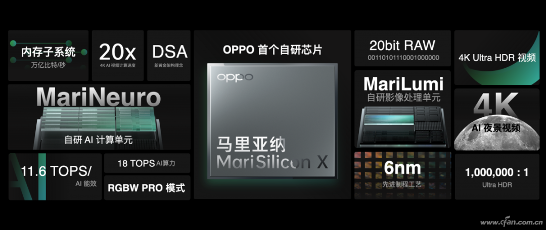
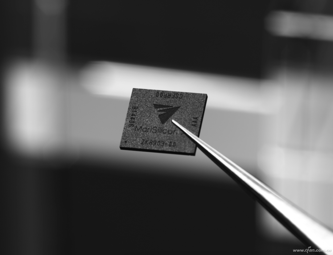
Yesterday, OPPO officially released its first self-developed NPU chip—MariSilicon X. This chip utilizes TSMC’s 6nm process and the new DSA architecture, integrating self-developed MariNeuro AI computing units and MariLumi image processing units, merging AI and image processing from the design stage, offering higher flexibility and performance compared to traditional ISPs, breaking the limits of mobile imaging capabilities through computational photography.Prior to this, Xiaomi and vivo also launched their self-developed ISP chips. The question arises, why are smartphone manufacturers so enthusiastic about ISP development now? How important is this module for imaging?
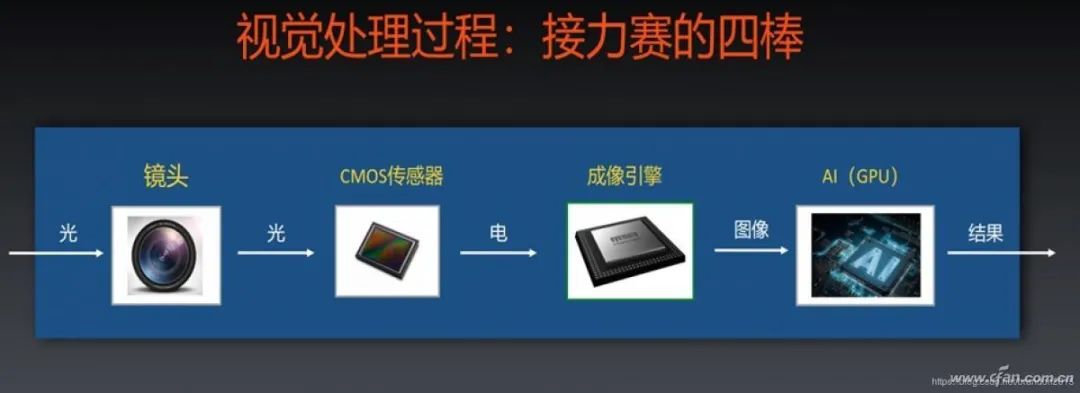
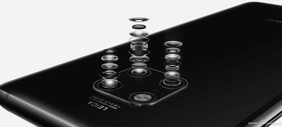
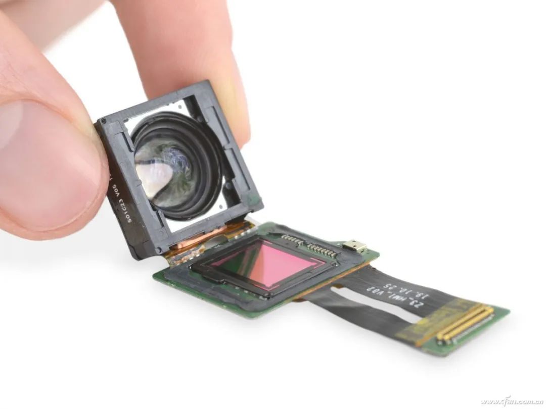
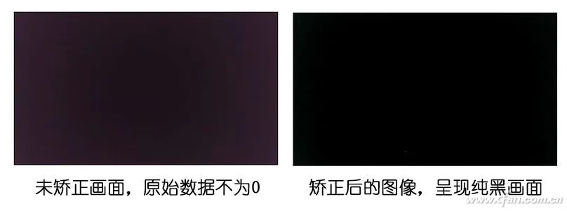
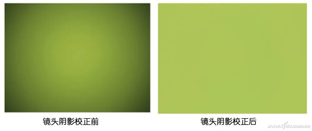
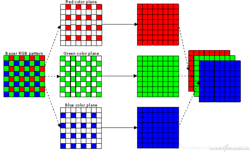
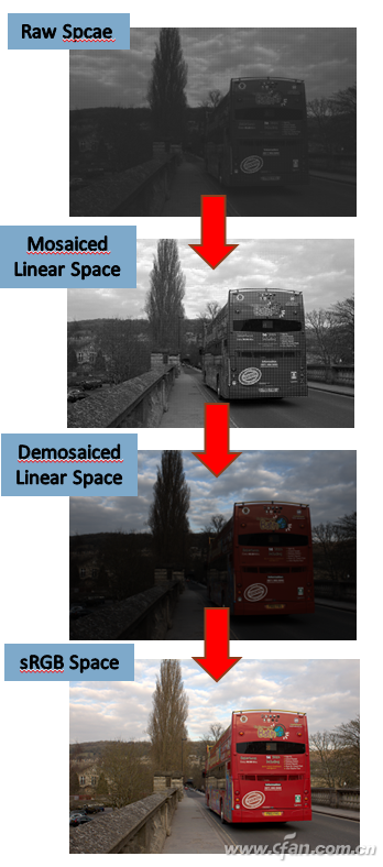
Simply put, the ISP (Image Signal Processor) is one of the core units in the mobile photography/videography process. The color and details of a photo or video ultimately depend on it.The Role of ISPWhen you press the (virtual) shutter of the mobile camera app to take a photo or record a video, you automatically enter a “relay race of visual processing.”First, light enters the camera module through the lens, passes through the IR Filter to filter out infrared light, and then reaches the CMOS sensor. At this point, the CMOS converts the optical signal into an electrical signal, which is then converted into a digital signal by the internal ADC circuit and transmitted to the ISP for processing. After undergoing a round of intelligent imaging algorithm optimization by the AI unit, it finally generates a visible image or video file.The question arises, when the lens and CMOS convert the optical signal into a digital signal composed of 0s and 1s, there may be omissions and errors in detail. The main task of the ISP unit is to perform “error correction,” “verification,” and “compensation.”This is similar to having you translate a Chinese idiom or proverb into English; the translator needs to have sufficient literary skills to accurately express the profound context of the Chinese in English. Indeed, at this moment, the ISP plays the role of the “translator.”ISP’s Compensation TasksThe lens of a smartphone consists of at least five lenses, optical devices, motors, gyroscopes, and other components, with “light transmittance” being an important indicator of lens performance.The main camera of a smartphone usually has more lenses than the secondary camera.CMOS is a core component, and factors such as sensor size, pixel size, RGGB or RYYB filter structure, unit pixel area, and multi-pixel fusion technology all affect its performance.In other words, both the lens and the sensor have physical defects, and continuous iterations from 7P to 8P lenses and from IMX586 to IMX700 CMOS can only approach perfection. This means that the original data (raw data) converted from them is imperfect.The larger the CMOS sensor size, the better its imaging foundation theoretically.On the other hand, when we take photos or record videos, the lighting conditions vary widely, requiring the lens and CMOS to adapt to the brightness and darkness of the environment like the pupil of the human eye.As the translator, the ISP’s main task is to optimize and compensate for the original data with physical defects and restore the brightness effects that meet our expectations, such as preventing overexposure in backlight situations and revealing details in low-light conditions. The ISP consists of many functional modules, and below we will briefly introduce the functional modules of the ISP and the parts that need compensation:BLC: Black Level CorrectionThe digital signal defines the original data of pure black as 0. However, due to the “leakage current” defect of CMOS, when the lens is placed in a pure black environment, the original data output from the lens and CMOS is not 0. At this point, the BLC (Black Level Correction) module in the ISP comes into play, obtaining a corrected result by subtracting characteristic correction values from all pixels. This process is known as black level correction, allowing the original data to display a pure black image.LSC: Lens Shade CorrectionDuring photography/videography, the light reaching the center of the CMOS from the lens is usually more than the light reaching the edges, resulting in higher brightness in the center of the image captured by the CMOS and lower brightness at the edges, which can easily lead to the so-called “vignetting” problem. At this point, the LSC (Lens Shade Correction) module within the ISP begins to intervene, detecting the areas where the brightness is more uniform in the image and calculating the compensation factors needed for the surrounding areas.Bayer Denoise: Noise Reduction ModuleIn addition to the ADC devices, the CMOS photo-sensing devices that contain an analog part also have some noise during signal transmission. The darker the shooting environment, the more the signal needs to be amplified, resulting in greater noise, which translates into the appearance of a large number of colored noise spots in the photo or video. The Bayer Denoise module in the ISP can significantly reduce the noise in the signal through multi-level filtering, thus minimizing imaging noise.BPC: Bad Point CorrectionCMOS sensors are physical devices, and over long-term use, it is inevitable that bad points will occur. The BPC (Bad Point Correction) module in the ISP automatically detects bad points and can replace the original values through median filtering, thus correcting bad points and preventing colored spots and bright spots from appearing in a completely black image or colored spots and black points from appearing in a pure white image.Demosaic: Color InterpolationThe CMOS sensor itself is actually “color blind.” If it only relies on its output, the photos will be black and white. To record colors, it needs to use a color filter array called Bayer (Bayer Color Filter Array, CFA) and overlay it on a photosensitive board. The structure of the Bayer color filter array mainly includes RGBW, RWWB, RGGB, and RYYB. However, since each pixel in the Bayer array can only capture one color channel’s information, the other two color information must be constructed through interpolation algorithms, combining the pixel information of other neighboring colors, which is somewhat similar to the process of “de-mosaicing.” This needs to be achieved by the Demosaic interpolation algorithm module within the ISP.AWB: Automatic White BalanceThe human visual system can self-correct; regardless of whether it is cloudy, sunny, indoors, outdoors, under incandescent light, or fluorescent light, it can accurately identify white without being affected by the color of the light source. However, the CMOS sensor does not possess this capability. A white paper will output color deviations under different light sources, such as low color temperature (like incandescent light) appearing yellow and high color temperature (outdoor sunlight) appearing blue. At this point, the AWB (Automatic White Balance) module in the ISP can automatically correct the color by detecting color temperature → calculating gain → color temperature correction, thus accurately recording white objects under different color temperature lighting.
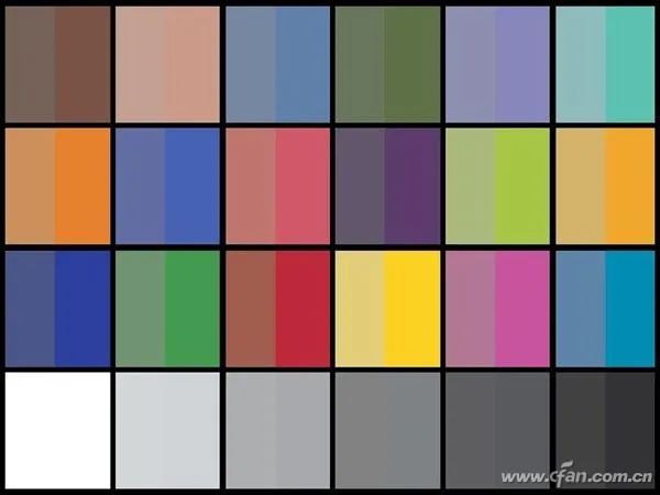
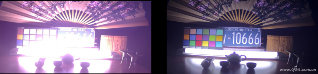
CCM: Color CorrectionDue to color penetration, there may be color errors between the color blocks of the CMOS sensor, leading to deviations between the images obtained by the CMOS and the expected colors. The previously mentioned AWB can correct white, while the CCM (Color Correction Matrix) module can calibrate the accuracy of other colors besides white, such as enhancing color saturation to make the image colors more vivid.AEC: Automatic ExposureThe intensity of light can change due to time and scene. The human eye has a certain adaptive ability to make timely adjustments according to changes in light intensity, but the CMOS sensor does not have this capability. Therefore, it is necessary to use the AEC (Automatic Exposure Control) module in the ISP to automatically adjust the exposure time based on light intensity and make certain exposure compensations when necessary.HDR: High Dynamic RangeThe intensity of light in nature is very wide, but the human eye’s ability to discern details in both bright and extremely dark environments is relatively narrow. The range that the CMOS sensor can record is even narrower, making it easy for the images output from the latter to lose details in bright and extremely dark areas. The HDR (High Dynamic Range) module in the ISP is designed for this purpose; it can reveal the lost image details in bright and extremely dark areas by using Tone Mapping to raise pixel values in particularly dark areas and lower them in particularly bright areas.In addition to the functions mentioned above, the ISP also includes modules such as RGB Gamma (gamma correction), RGBToYUV (color space conversion), Color Denoise/Sharpness (color noise reduction/sharpening), and Auto Focus (automatic focusing). It is important to note that the above are only the basic functions of the ISP; different ISPs (including independent chips and SoC integrated ISP modules) may introduce unique or stronger features.Although Qualcomm Snapdragon and MediaTek Dimensity 5G SoCs have already integrated performance-capable general ISPs, they are difficult to match 100% with the smartphone manufacturers’ own AI algorithms. Therefore, developing self-research ISPs (NPU) to match their own AI algorithms has naturally become a breakthrough path for smartphone manufacturers, allowing them to achieve imaging effects that are more pleasing to users’ aesthetics in the face of hardware homogenization.
Click “Read Original” to see more exciting content