In the previous issue, we introduced some background knowledge about chip packaging:A Beginner’s Guide to Chip PackagingIn this issue, we will focus on the specific process of packaging.As previously mentioned, there are many forms of packaging, including traditional and advanced packaging.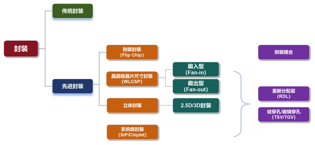 Different packaging types have different processes and techniques. After completing the entire write-up, I found it too lengthy (over 10,000 words). To reduce reading difficulty, I decided to split it into two parts (Traditional Packaging and Advanced Packaging).Today, we will first publish theTraditional Packaging.█ The Process of Traditional PackagingThe general process of traditional packaging is as follows:
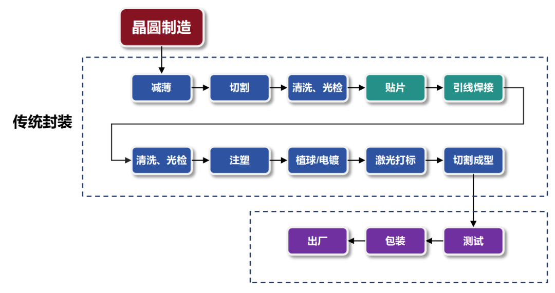 Let’s take a look at each step.· ThinningThe first step in traditional packaging is thinning the wafer—reducing the thickness of the wafer (fromoriginally600–800μm down to tens to a hundredμm, or even thinner).
 The main purposes of thinning are threefold:First, to reduce the chip size to meet packaging requirements.Second, to achieve better heat dissipation.Third, to enhance electrical performance and reduce parasitic effects (excessive thickness increases parasitic capacitance and signal transmission delay) and conduction resistance.Thinning also requires caution to avoid affecting the mechanical strength of the wafer, as this may lead to breakage during subsequent processes. Additionally, thermal stress generated during thinning may cause the wafer to warp or be scrapped.The current thinning process employs the CMP (Chemical Mechanical Polishing) technique mentioned in the wafer manufacturing section.
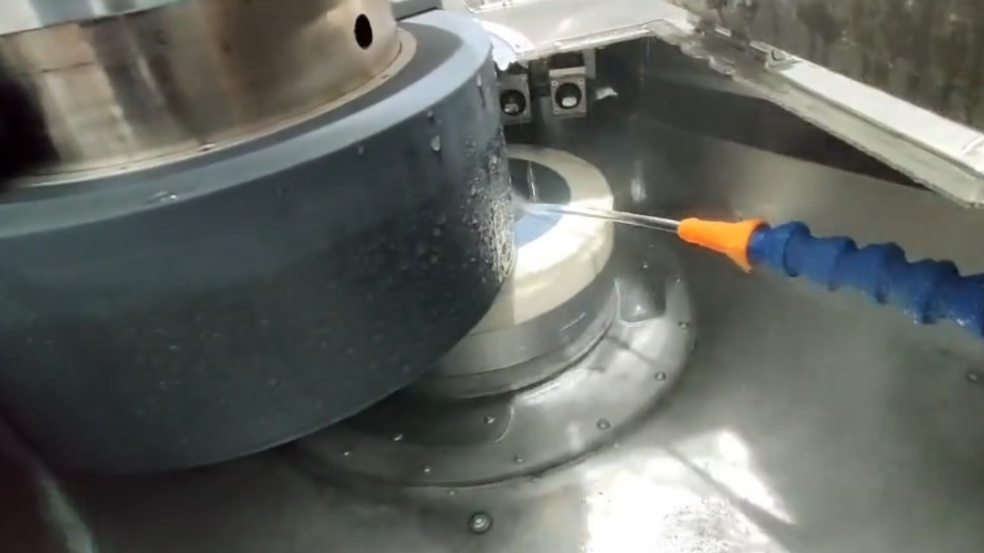 Thinning in progress· Dicing (Cutting, Sawing, Scribing)After thinning, we begin the formal cutting (Dicing).Before cutting, a protective blue film is applied to the front of the wafer to prevent damage to the chips during the cutting process.The wafer is very fragile. As time goes on, the precision of chips increases, and the gaps between chips on the wafer become smaller, raising the requirements for cutting technology.The commonly used cutting method in the past wasmechanical cutting. By using a high-speed rotating ultra-thin diamond blade, cutting can be completed along pre-defined grooves on the wafer (i.e., wafer scribing).During the cutting process, pure water is used for cooling and to remove debris.Mechanical cutting is relatively simple and cost-effective, but it has low precision, slow speed, and is prone to chipping, so it has gradually been phased out.
 Later,laser cutting was developed, which uses high-energy laser beams for cutting.Laser cutting can be divided into full cutting and hidden cutting.Full cutting: The laser beam directly hits the surface of the wafer, penetrating the entire thickness of the wafer, completely severing it. This method has an extremely fast cutting rate but generates debris and heat, requiring cleanup and cooling.Hidden cutting: This involves two steps. First, the laser beam focuses on the interior of the wafer, creating fine cracks inside while keeping the surface intact. Then, mechanical means are used to uniformly stretch the tape attached to the back of the wafer. As the tape expands, individual chips on the wafer separate along the pre-cut laser path, completing the cutting process.Laser hidden cutting avoids the thermal damage issues of traditional laser cutting, making it very suitable for high-speed and high-quality cutting of ultra-thin semiconductor wafers.
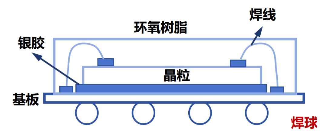
 Subsequently,plasma cutting was introduced.It works by ionizing gas to react with silicon in the cutting path, completing the cut.Plasma cutting is fast and causes minimal damage, making it particularly suitable for cutting ultra-small chips. It can also reduce the width of the cutting path, increasing the number of chips designed on the wafer, further lowering chip costs.· Die AttachAfter cutting the chips, die attach is required.In traditional packaging, die attach involves bonding the chip to the packaging substrate (Substrate).The packaging substrate, also known as the IC carrier board, is a special type of PCB (Printed Circuit Board).It features high density, high precision, and lightweight characteristics, providing support, connection, heat dissipation, and protection for the chip.Common bonding methods in traditional packaging includeadhesive bonding,welding bonding, andeutectic bonding.Epoxy resin is a commonly used organic adhesive. It achieves bonding through thermal curing.Epoxy resin is inherently insulating, but when mixed with a certain proportion of silver powder, it gains conductive properties, becoming conductive adhesive, also known as silver glue, which is more widely used.
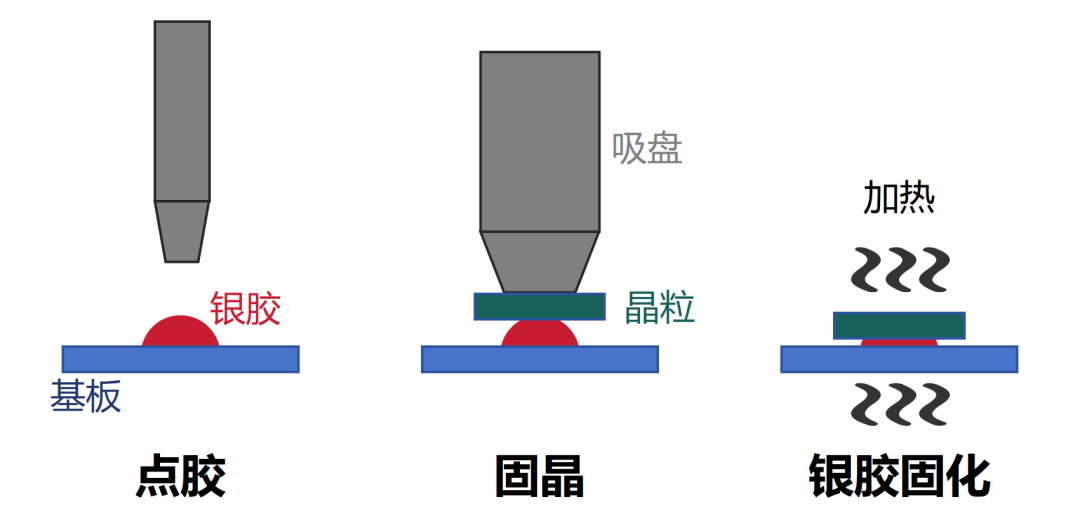 Welding bonding is achieved through molten solder to connect the chip and substrate, including softsoldering (using low-melting-point solder, such as tin-lead alloy) andhard soldering (using high-melting-point solder, such as gold-silicon alloy).Eutectic bonding utilizes two or more metals to form an eutectic alloy at the eutectic temperature to achieve connection.It has high connection strength and good thermal conductivity, but the process is complex and costly.
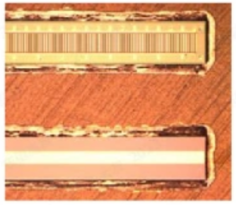 Eutectic bondingDie attach requires the use of die attach machines. There are many types of die attach machines, including SMT die attach machines and advanced packaging die attach machines.Die attach has high precision requirements; even a small deviation can cause the chip to malfunction.During the die attach process, potential mechanical damage and thermal conduction issues caused by the die attach materials must also be considered (which may hinder normal heat dissipation).(A reminder: this article discusses traditional packaging. Currently, advanced packaging is widely used, and the processes differ significantly. Please do not apply traditional methods to advanced packaging.)· Wire BondingAfter die attach, electrical connections between the chip and substrate must be established.Traditional packaging connects using metal wires, hence the term wire bonding process.
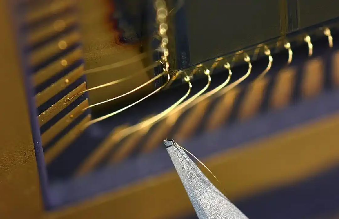 Wire bondingDuring the bonding process, heat, pressure, and ultrasonic energy are applied to break the surface oxide layer and contaminants, causing plastic deformation to ensure intimate contact at the interface, forming stable bonding points through electron sharing and atomic diffusion.
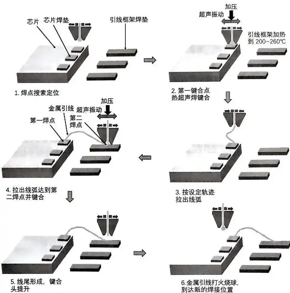 Thermal ultrasonic welding processThe materials used for wire bonding are generally gold, silver, copper, and aluminum.Gold has excellent conductivity, stable chemical properties, fast ball bonding speed, oxidation resistance, and does not react with acids and bases, but it is expensive, and its usage share is continuously declining.Silver is cheaper than gold but still somewhat expensive.Aluminum, while lower in cost, has poorer stability and lower yield rates.Copper has a balanced cost and performance and is currently widely used (especially in mid-to-low-end products).
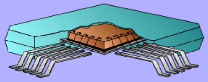
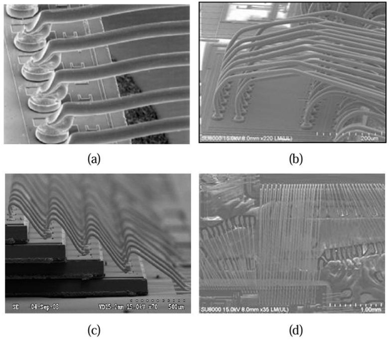 Example of high-density leads· Cleaning and Optical InspectionCleaning is self-explanatory.For inspection, in addition to using low-magnification microscopes to check the product’s appearance, AOI (Automated Optical Inspection) can also be performed.
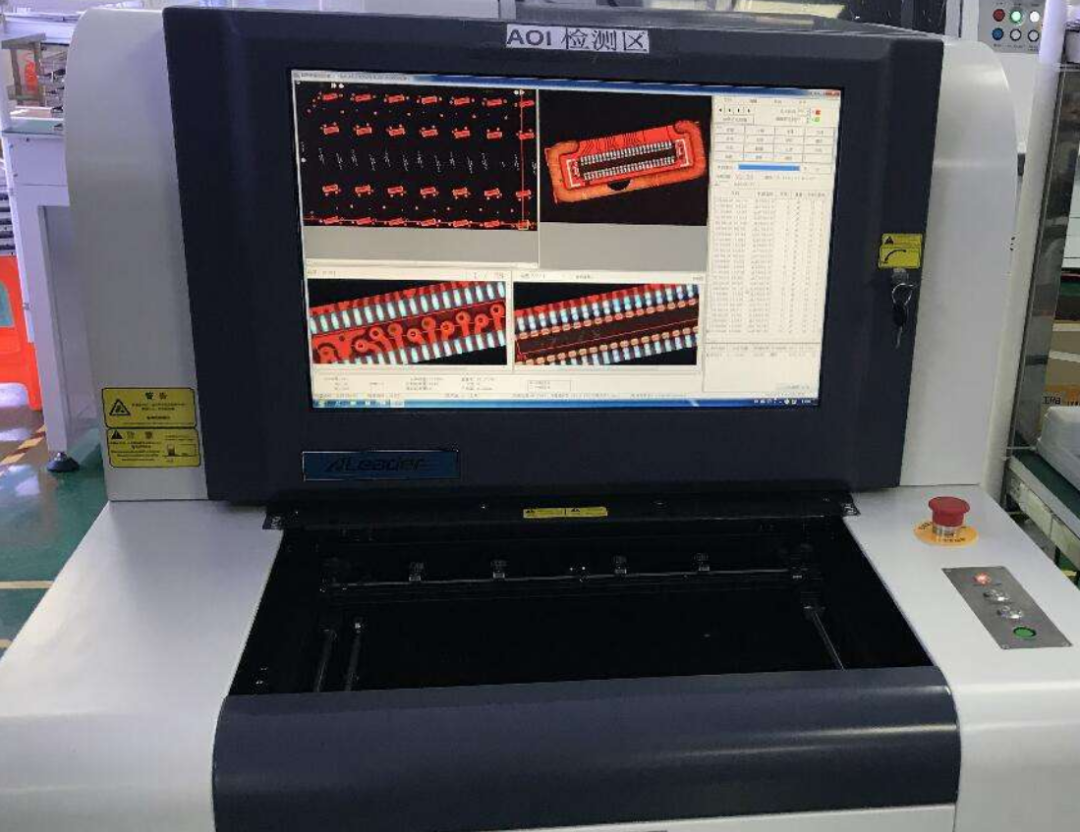 AOI InspectionAOI has three significant advantages:First, it has exceptionally high detection efficiency, capable of inspecting hundreds of components per minute.Second, it has quantifiable detection capabilities, recording defect sizes, locations, and other data, facilitating process traceability and improvement.Third, it can detect microscopic defects that are difficult for the human eye to identify, such as weak solder joints and micro-cracks.In the semiconductor packaging field, AOI is generally performed four times (four stages).The first optical inspection is for wafer inspection, the second is for particle appearance defect detection, the third is for die attach/wire bonding inspection (which is the current topic), and the fourth is for plastic encapsulation appearance inspection (to be done later).· Molding (Plastic Encapsulation, Injection Molding)Next, we proceed to molding.It is important to note that packaging can be divided intoplastic packaging,ceramic packaging, andmetal packaging based on the materials used.
Ceramic and metal packaging have good sealing and heat dissipation properties but are expensive and have long production cycles, so they are mainly used in aerospace and military fields.
Plastic packaging has relatively poor heat dissipation, stability, and airtightness, but it is lightweight, compact, and inexpensive, making it the mainstream choice in civilian commercial fields.
In China, over 90% of semiconductor packaging uses plastic packaging. Among plastic packaging, over 97% utilizes epoxy molding compound (EMC) as the encapsulation material.Epoxy molding compound (EMC) is a thermosetting chemical material used for semiconductor packaging. It effectively protects the chip from external environmental influences (moisture, temperature, pollution, etc.) and achieves composite functions such as heat conduction, insulation, moisture resistance, pressure resistance, and support.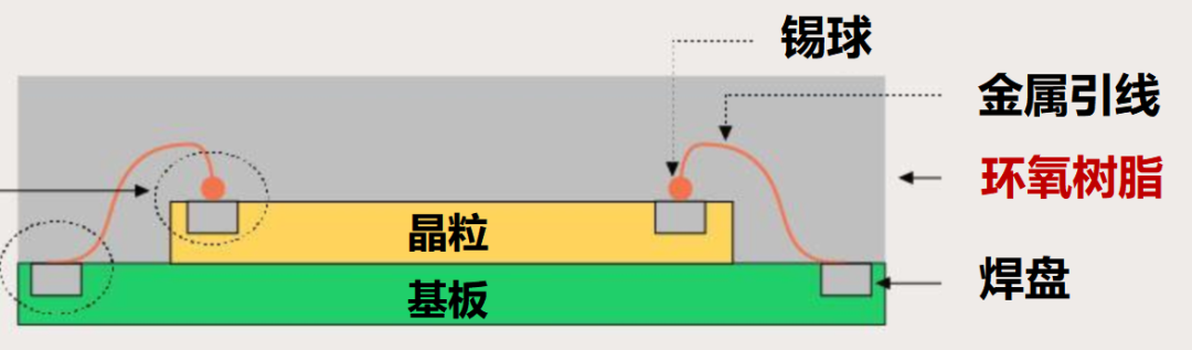 Molding can be performed using transfer molding and liquid encapsulation processes. The former involves melting the epoxy resin molding compound and injecting it into a mold under pressure and temperature to encapsulate the bare chip. The latter is mainly used for ultra-thin or flexible packaging.To ensure the stability and safety of the chip, a metal protective cover may be installed on it under certain special requirements, a process known as Lid Attach. This protective cover is usually made of alloys with excellent heat dissipation properties.
 · De-flashing (Removing Flash)After molding, a de-flashing process is required to remove the excess material around the chip.The de-flashing method mainly involves weak acid soaking and high-pressure water washing.· Post-Mold CureAfter de-flashing, the post-mold cure process is performed, baking at 150–180°C for several hours to fully cure the molding material and enhance mechanical strength.· Ball PlacementFor BGA (Ball Grid Array) packaging in traditional packaging, solder balls (tin balls) must be precisely placed on the chip surface to achieve electrical connections between the chip and the circuit board. This process is called ball placement.
 This ball is not directly soldered onto the substrate; solder paste or flux is used.First, solder paste is printed onto the pads, and then solder balls of a certain size are added on top. At this point, the solder paste will hold the solder balls. By heating, the contact area of the solder balls is increased, allowing for faster and more comprehensive heating. This improves the solderability of the solder balls when melted, reducing the likelihood of cold solder joints.(In the next issue, when we discuss advanced packaging bumping processes, we will revisit solder balls.)· Plating (Tin Dipping)To enhance the conductivity, solderability, and corrosion resistance of the pins, and to reduce the impact of external environmental humidity and heat, a layer of materials such as tin, nickel, palladium, or gold is plated onto the pins using metal and chemical methods.Due to EU RoHS requirements, lead-free plating is generally used, employing 99.95% high-purity tin.Products plated without lead are required to be baked at high temperatures for a period (annealing) to eliminate potential whisker growth issues in the plating layer.· Trimming and Forming (Bending)Excess frame material is removed. For packaging types with leads (such as SOP, QFP), the leads need to be bent into standard shapes.
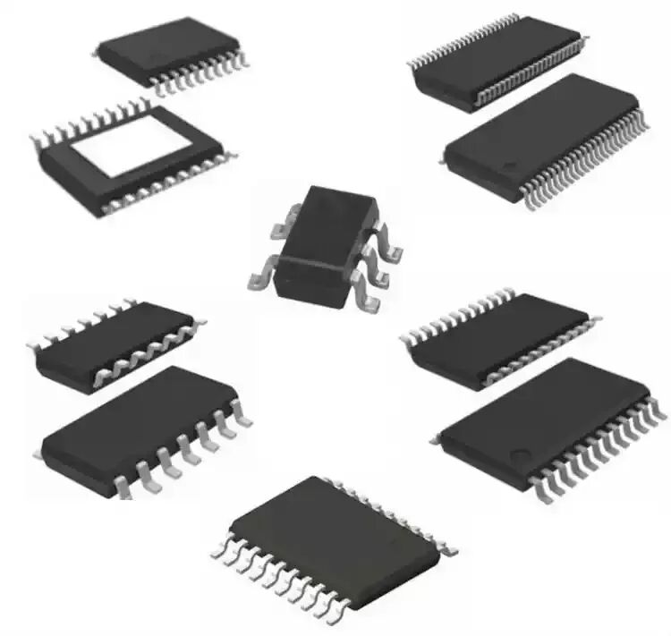
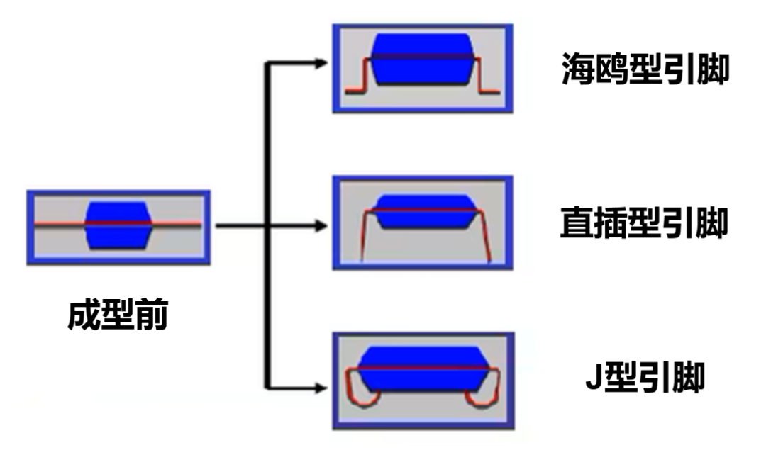
 · Final TestingAfter packaging is complete, testing is conducted again.The testing before the packaging process is called wafer testing (CP, Circuit Probing),also known as mid-testing.The testing after the packaging process is called final testing (FT, Final Test),also known as end testing.Final testing involves comprehensive testing of the packaged chip for application in devices. This is a crucial step aimed at ensuring that the chip meets expected standards for functionality and quality before shipment.Similar to CP testing, FT testing also relies on ATE (Automated Test Equipment) along with test boards and sorting machines to ensure accuracy and efficiency in testing.To compensate for the shortcomings of ATE testing in complexity and fault coverage, SLT (System Level Test) is also introduced.SLT testing is designed based on the actual application scenarios of the chip, aiming to simulate real business flow environments through carefully crafted test boards and rigorous testing processes, thereby reducing the defect rate of chip products and enhancing user trust.· MarkingAfter testing, marking can be done.Using laser printing, information such as the chip manufacturer’s logo, product name, and production batch is printed on the chip surface for easy identification during subsequent use.
 · ShippingAccording to customer requirements, the tested products are classified and packaged from standard containers into customer-specified packaging containers, with necessary labels affixed, ready for shipment.They may be for retail or sent to OEM manufacturers.Thus, the process of traditional packaging is complete!Get ready; in the next issue, we will look at the complex advanced packaging!References:1. “Complete Process Flow of Chip Manufacturing”, Semiconductor Packaging Engineer’s Home;2. “Understanding the Chip Production Process in One Article”, Eleanor Wool Sweater;3. “Must-Read Complete Process Flow of Chip Manufacturing”, RF Academy;4. “Understanding Wire Bonding”, Failure Analysis Engineer Zhao;5. “An Important Direction of Moore’s Law, Advanced Packaging Has Great Potential”, Huafu Securities;6. “Introduction to the Reasons, Sizes, and Four Thinning Methods for Wafer Thinning”, Tom Talks Chip Manufacturing;7. Wikipedia, Baidu Encyclopedia, various manufacturers’ official websites.