How Did the Number of Transistors in Chips Reach Today?

Source: Content from cpuTECH and ECO, thank you.
Beginning with the birth of the Intel 4004, the fifty-year history of microprocessors has been written. Few fields have developed as rapidly as microprocessors, which have advanced across seven orders of magnitude in just fifty years—from 2,300 transistors to 54 billion. The initial 4-bit single ALU design has evolved into multi-core behemoths, powering nearly every aspect of human life.
To illustrate these changes, MPR highlights several products that define the entire industry, including the Intel 8088, MIPS R2000, DEC Alpha 21164, Intel Core Duo, IBM Power8, and Nvidia A100. Each product demonstrates increasing performance through upgrades in frequency and microarchitecture.
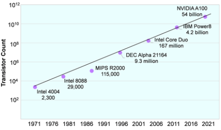
Over the past 50 years, the rise in transistor count has astonishingly aligned with Gordon Moore’s prediction (Moore’s Law), which states that the number of transistors doubles approximately every two years. Applying this doubling rate to the transistors of the 4004 predicts that processors with 54 billion transistors would appear by 2020, as illustrated in Figure 1, which Nvidia achieved with the A100. Although transistor count remains closely related to performance, companies have also improved performance through innovations in circuit structure and microarchitecture during this period.
How Did the Number of Transistors in Chips Reach Today?
Figure 1 Transistor Count Over 50 Years
(According to Moore’s Law, this number doubles steadily every two years. Nvidia’s A100, a chip reaching the reticle-size limit, perfectly matches this prediction. (Data source: various manufacturers))

A One-Man Army Releases the 4004

Intel released its 4-bit 4004 processor in 1971, manufactured with a 10-micron process on a two-inch wafer. Compared to earlier integrated circuits with dozens or hundreds of transistors, it was the most advanced design at the time, including 2,250 transistors. However, it was created by a single engineer, Federico Faggin, who worked 80 hours a week to deliver the 740kHz processor on time (see MPR 12/18/06, “35th Anniversary of the Intel 4004”). In addition to designing the logic and circuits, he also had to manually cut the ruby film used to create the optical masks. In a moment of self-indulgence, the designer etched “F.F.” on one mask.
The 4004 implemented only 46 instructions, five of which were double-length. The processor integrated a single ALU, completing 4-bit additions (and most other instructions) in eight clock cycles, resulting in an effective execution rate of less than 0.1MHz. Despite having a complete CPU with a size of 12 square millimeters, the 4004 could not operate independently, as it lacked any memory aside from a 64-bit (16×4-bit) register file. Therefore, Faggin also delivered the 4001 ROM chip, the 4002 bus interface chip, the 4002 RAM chip, and the 4003 bus interface chip.
The 4004 revolutionized the market as the first software-programmable chip. It initially served Busicom’s 141-PF calculator, as that company held exclusive rights to the design. However, Intel realized that programmability made this design suitable for a wide range of systems, so it negotiated an agreement allowing Intel to sell the 4004 to other customers, thus pioneering the microprocessor market. Even in 1971, the company was eyeing the gaming market; for example, the 4004 eventually made its way into pinball machines, adding a touch of sophistication to once purely mechanical games.

8088 Powers the IBM PC

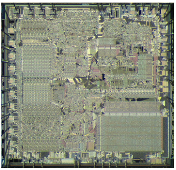
The 16-bit Intel 8088 was launched in 1979. As shown in Figure 2, the company manufactured this chip, which contains 29,000 transistors, using its 3-micron technology. The peak speed hovered around 5MHz. Intel created the 8088 in its newly established Haifa laboratory in Israel. The processor was fundamentally the same as the 8086, which introduced the x86 instruction set, but the 8088 reduced the external bus interface to 8 bits to lower system costs. Like the 8086, it featured a 6-byte instruction queue, a 16-bit ALU, and 16-bit registers. Its simple pipeline had two segments: instruction fetch/decode and execution.
How Did the Number of Transistors in Chips Reach Today?
Figure 2 Photo of AMD’s 8088 Chip Die
(The 8088 has a die size of 33 square millimeters and 29,000 transistors. Although the chip was initially designed by Intel, many similar manufacturers like AMD obtained design licenses to manufacture it. (Photo source: Pauli Rautakorpi, Wikipedia , licensed under CC BY 3.0))
However, compared to the 8086, the 8088 suffered from performance issues due to its narrower data bus and smaller prefetch queue. It embodied the inefficiencies of sequential processors: for example, programmers needed to interleave long and short instructions to avoid bottlenecks. The 8088 also had difficulties with calls, jumps, and interrupts, as these instructions reset the prefetch queue, which could take 15 cycles to refill. The 4004 required custom memory chips, while the 8088 could use off-the-shelf RAM and ROM. Customers often paired the 8088 with Intel’s 8-bit latch 8282 processor, the 8284 clock generator, the 8-bit 8287 driver, the 8288 bus controller, the 8259 bus arbiter, and the 8087 math coprocessor.
The 8088 won a significant design in the first IBM PC, ensuring Intel and the x86 architecture’s long-term central position in the personal computer revolution. Intel was not the only company offering 8088 solutions; IBM required a second source of supply, so Intel licensed the 8088 design to AMD, NEC, Texas Instruments, and others. During this period, licensed processors were common, but Intel eventually ceased this practice with the 80386 era in 1985.

MIPS Provides the First RISC Processor

MIPS Computer Systems provided the first commercial implementation of MIPS ISA in 1986, shaking the computer architecture world. The R2000 was the first commercialized RISC architecture, sparking the RISC versus CISC debate. This 32-bit chip with 110,000 transistors came in three speed grades: 8.3MHz, 12.5MHz, and 15MHz. MIPS was among the first processor suppliers without a fabrication line, outsourcing the R2000 to Sierra Semiconductor and using its 2-micron dual-layer metal CMOS process (see MPR 2/89, “MIPS Challenges SPARC and 88000”).
The execution engine of the R2000 featured an ALU and a multiplication/division unit. The simplified RISC architecture processed one instruction per clock cycle, far surpassing competitive CISC processors. The CPU had five pipeline stages, making it a template for sequential RISC designs for decades to come, including RISC-V’s Rocket CPU. Like its contemporary 80386, the R2000 required external chips for high-speed caching and (optionally) executing floating-point (FP) operations.
The R2000 was particularly popular among workstation and server manufacturers. Its robust mathematical performance made MIPS an ideal choice for engineers and scientists, while its ISA became increasingly popular due to its optimized software stack. Compiler designers helped create one of the earliest ISA simulators, accelerating the adoption of UNIX on MIPS machines.

DEC Overwhelms Intel on Performance

As shown in Figure 3, the Alpha 21164 was a beast of a microprocessor. Digital Equipment Corporation (DEC) released it in 1994, with a maximum frequency of 300MHz (see MPR 9/12/94, “Digital Leads the Way with 21164”). The seven-stage pipeline was deeper than any competitor’s design, giving the processor a speed advantage. The 21164 implemented DEC’s proprietary 64-bit Alpha architecture, supporting UNIX and OpenVMS. The company manufactured the chip using its 0.5-micron process, cramming in 9.3 million transistors.
How Did the Number of Transistors in Chips Reach Today?
Figure 3 Photo of DEC’s Alpha 21264 Chip Die
(This chip was a giant at the time, measuring 314 square millimeters. With a clock speed of 300MHz, it far surpassed other competing chips. (Photo source: Pauli Rautakorpi, Wikipedia , licensed under CC BY 3.0))
The superscalar microarchitecture of the 21164 was similar to recent processors. It integrated an 8KB instruction cache and passed instructions to a width-4 decoder, which issued four decoded instructions to the execution engine each cycle. The 21164 included two integer units and two floating-point units for arithmetic operations. It also implemented an on-chip secondary cache with a capacity of 96KB. The design featured a 43-bit virtual address space and a 40-bit physical address space, allowing it to handle more memory than its contemporaries—8TB of virtual memory and 1TB of DRAM. This address space provided unique advantages for applications requiring large datasets.
Upon its release, the 21164 expanded DEC’s performance lead: it scored 15.4 in SPECint95 and 21.1 in SPECfp95, surpassing Intel’s Pentium in both respects. Systems powered by the Alpha 21164 achieved new feats such as CAD modeling, multimedia editing, and even video conferencing. In 1994, DEC was at the pinnacle of the world, as its Alpha lineup offered unmatched performance. However, when Intel’s Pentium Pro (P6) arrived, the good times ended, as it used RISC technology to enhance x86 performance. From that point on, RISC’s popularity in PCs and servers plummeted, leading DEC to abandon Alpha in 2001.

Core Duo is the First Multi-Core PC Processor

Intel released the Core Duo in 2006, the first multi-core personal computer processor. Servers had already adopted multi-core chips, but the company brought this approach to personal computers, offering two different designs for laptops and desktops (see MPR 10/3/05, “Yonah Gets Multi-Core Right”). The company manufactured the desktop version (Conroe) with a die area of 143 square millimeters on its 65-nanometer node, packing 291 million transistors. It reached frequencies of up to 3.0GHz while running both 32-bit and 64-bit x86 architectures. Following Intel’s high-frequency NetBurst approach, Conroe was one of the first processors to utilize the Core microarchitecture, which still forms the basis of the company’s current flagship CPUs.
The Core Duo initiated today’s multi-core movement and became central to it. By placing two CPUs on a single die to fill its transistor budget, Intel significantly boosted performance. Another option would have been to build a more complex single-core CPU, which would have doubled in size relative to the previous generation, but this proved impractical. The out-of-order Core CPU cores integrated a 32KB instruction and data cache, four decoders, a 96-entry reorder buffer, and five execution ports for memory and arithmetic operations. It integrated a 128-bit SIMD unit to accelerate Intel’s vector (SSE) extensions.
The new dual-core processor was notable not only for its performance but also for its (at the time) impressive 65W TDP power rating. However, dual-core mode posed challenges for software designed to run on a single CPU. Engineers needed to implement multi-threading programming models. Updated software took years to release; during this period, few users could see the promised performance gains.

Power8 Takes Multi-Threading to a New Level
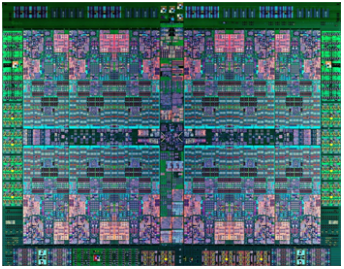
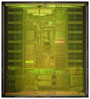
By 2014, multi-threaded software had become the norm, but Power8 took multi-threading to a new level. Released in 2014, it was a multi-threading monster, packing 12 cores with 96 threads (see MPR 12/29/14, “Power8 Shocks the Commercial Market”). IBM manufactured this 190W chip using 22-nanometer silicon-on-insulator (SOI) technology. Even by modern standards, it was enormous, with a die area of 650mm² and containing 4.2 billion transistors, as shown in Figure 4. It was also the first POWER chip available for commercial purchase.
How Did the Number of Transistors in Chips Reach Today?
Figure 4 Photo of Power8 Chip Die
(In 2014, IBM advanced multi-threading to new heights with 12 cores, each with 4 threads. The 22-nanometer die size was 650 square millimeters while packing 4.2 billion transistors. (Photo of the die taken by IBM))
When designing Power8, on-chip memory became a focus for IBM. The chip featured 512KB of secondary cache per core and 96MB of embedded DRAM (eDRAM) for L3 cache. The use of eDRAM was unique: it allowed IBM to integrate a large amount of memory on the chip, which would have been impossible with SRAM alone. Even with a massive number of cores, Power8 achieved speeds of up to 3.6GHz. The design featured a particularly wide execution engine with 14 execution units, capable of handling branches as well as integer, floating-point, fixed-point, and vector operations. The extensive execution engine helped Power8 surpass competitors in IPC.
This processor still allowed Intel to profit in the server market. The Power8 was priced 30% lower than Intel’s flagship Xeon E5-2699v3 while offering similar integer performance and leading floating-point performance. Global bankers and retailers benefited from the fixed-point decimal engine, which accelerated traditional Cobol software. Despite better performance and lower pricing, the processor lacked x86 compatibility, limiting its appeal outside of IBM’s own systems.

Nvidia A100 Reaches the Reticle Limit

Nvidia’s A100 best represents today’s high-performance processors, achieving leading performance in a popular application using a specialized architecture. The company’s GPUs have become synonymous with neural network training (see MPR 6/8/20, “Nvidia A100 Leads in AI Performance”). Over the past decade, the proliferation of AI applications has skyrocketed, touching many aspects of daily life. However, the immense computational demands brought by neural networks have created a demand for specialized hardware. The A100 GPU, designed for data centers with a power consumption of 400W, went into mass production in the second quarter of 2020 and immediately became a hot product in AI. It features 54 billion transistors; the massive 826mm chip tests TSMC’s reticle size limits in 7-nanometer technology.
The A100 implements Nvidia’s Ampere GPU architecture to accelerate AI training and inference. The VLIW configuration reduces instruction scheduling logic, and many SIMD units benefit the large convolutions often employed in neural networks. The chip has 108 GPU cores and includes matrix multiplication units and vector ALUs. Its release positioned Nvidia at the top of the AI market. The company built a massive software ecosystem around the A100 and other GPU-based AI accelerators, targeting nearly every conceivable field, from healthcare to agriculture to molecular dynamics.

The Victory of Moore’s Law

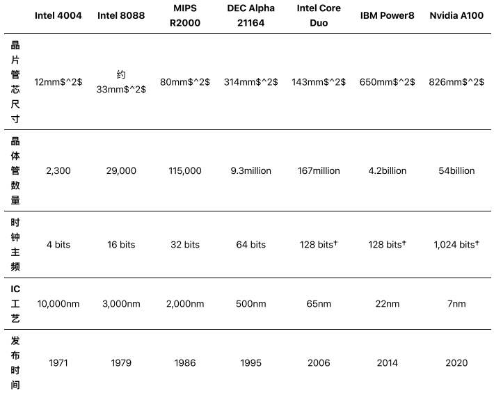
As shown in Table 1, the number of transistors on a single chip has explosively increased over the past 50 years. Each product in the table required significant technological advancements, from optical lithography to ultraviolet, multi-patterning, and today’s EUV (see MPR 5/20/19, “EUV Technology Reaches Volume Production”). Transistor area has decreased by 2 million times. As defect rates have decreased and processes have improved, die sizes have also increased, allowing for more transistors on each chip. These factors have enabled more complex microarchitectures, more on-chip memory, and ultimately more cores per chip, enhancing performance.
How Did the Number of Transistors in Chips Reach Today?
Table 1 Historical MPU Comparison
(Over 50 years, the number of transistors has surged. This growth has been made possible by advancements in mainstream process technologies. † SIMD units were used. (Source: manufacturers))
For CPU-based processors, frequencies have increased by four orders of magnitude. The 4004 started at less than 1MHz, but modern Intel processors can reach 5,200MHz. CPU designers have employed two techniques to increase clock frequencies: one relies on foundries to enhance transistor speed, while the other achieves gains through microarchitecture upgrades.
Although the A100 is a GPU, MPR still considers it a processor because it loads and executes instructions. MPR includes Nvidia’s chip to emphasize how GPUs and AI products are now driving Moore’s Law. Cutting-edge designs have hundreds of 1,024-bit ALUs, a far cry from the single 4-bit ALU on the original microprocessor.

How Did We Get Here Today?

No single article can cover the entire 50-year history of microprocessors. MPR’s curated selection includes products it considers representative during this time period, highlighting the many structural changes the processors have undergone. The earliest examples could only perform the most basic functions, such as addition, and lacked on-chip memory. Over time, designers integrated additional functionalities, such as floating-point units and bus interfaces, which were previously on separate chips.
Once the entire CPU was on a chip, companies began adding more CPUs. Data paths expanded from 4 bits to 64 bits, and even wider for specialized SIMD units (consuming many transistors in the process). Caching began as an external feature in the 1980s, transitioned onto chips in the 1990s, and evolved into today’s complex multi-level caches. Deeper pipelines achieved higher clock speeds, but they required more buffers and bypass logic, further increasing transistor counts.
While techniques like deeper pipelines and wider execution units seem to have reached their limits, chip designers are still attempting to improve performance through different approaches, such as specialized applications and heterogeneous architectures. When they lack better ideas, they add more CPU cores, though few PC applications can utilize them.
Relative to the span of human history, 50 years is nearly a blip. Yet in this insignificant period, the development speed of microprocessors is astonishing. They are ubiquitous, from microwaves to self-driving cars. When people take time to appreciate microprocessors, they must also remember how this valuable invention started from the humble 4004.
How Did the Number of Transistors in Chips Reach Today?

Leave a Comment