In the previous article titled “The Convergence Point of PCB Manufacturing Technology Upgrades in the AI-PCB Industry Chain: Copper Clad Laminate (CCL)”, it was mentioned that Copper Clad Laminate (CCL) is the core substrate of printed circuit boards (PCBs).CCL is made from an insulating resin matrix, reinforced materials (such as glass cloth and paper base) as the framework, and one or more layers of copper foil coated on the surface or inside, formed through hot pressing.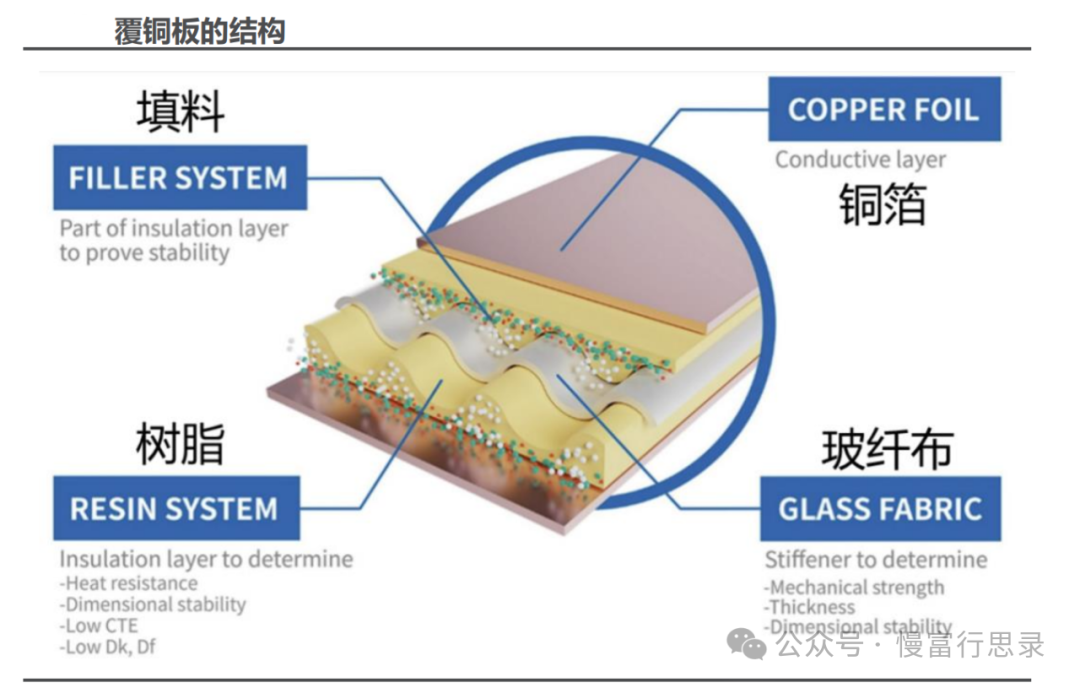 The largest direct cost in PCB production is the copper clad laminate, with the cost of copper foil accounting for the highest proportion at 42.1%, while resin and glass fiber cloth account for 26.1% and 19.1%, respectively.1. Copper Foil1) According to the production process, it can be divided into:① Electrolytic Copper Foil: Copper foil formed by electro-deposition on the cathode roller, which has a lower manufacturing cost but a relatively rough surface, suitable for mass production.② Rolled Copper Foil: Copper ingots rolled into thin sheets through a rolling mill, which has better ductility and surface smoothness, suitable for flexible circuit boards and high-frequency circuits.2) According to performance, it can be divided into: standard PCB copper foil and high-performance PCB copper foil.High-performance PCB copper foilcan be classified into five categories: high-frequency and high-speed circuit copper foil (HVLP is currently the highest-end product), ultra-thin copper foil for IC packaging substrates (PUTCF is the highest-end product), copper foil for high-density interconnect circuits (HDI), thick copper foil for high-power and high-current circuits, and copper foil for flexible circuit boards.① HVLP also known ashigh-frequency ultra-low profile copper foil, has advantages such as high hardness, smooth surface, uniform thickness, stable and efficient current transmission, and low signal loss, making it widely applicable in fields with high signal transmission requirements such as AI servers, smart vehicles, communication devices, consumer electronics, and aerospace.HVLP copper foil can be divided into generations 1-5 based on roughness. Currently, HVLP1 and HVLP2 are the most common, while some AI products with high electrical performance requirements have upgraded to HVLP3 and HVLP4 copper foil, and HVLP5 has the highest technical threshold, positioned as the next-generation product, not yet in mass application.
② Peelable Ultra-Thin Copper Foil (PUTCF), referred to as peelable copper, refers to copper foil with a thickness of less than 9μm, supported by a carrier, characterized by high tensile strength, good thermal stability, and low surface profile, suitable for producing chip packaging substrates.
During use, it can be peeled off, suitable for the mSAP semi-additive process and Coreless process in PCB manufacturing, significantly reducing the thickness and weight of PCBs and IC substrates, meeting the demand for lightweight and thin terminal electronic products.
High-speed copper foil and peelable copper technology have high barriers to entry, previously monopolized by overseas companies from Japan and South Korea.Domestic manufacturers are truly accelerating their layout, and in the future, they are expected to leverage the domestic AI industry chain to achieve a leapfrog development.Defu Technology (301511) has announced a preliminary intention to acquireHVLP3 and peelable copper products that have been successfully applied in AI products from Luxembourg copper foil.Copper Crown Copper Foil (301217) has the production capacity for HVLP1-4 generations, with the second generation being the main shipment.Longyang Electronics (301389) is currently validating HVLP5 copper foil with customers, expected to grasp future directions.Fangbang Co., Ltd. (688020) also has deep technical reserves in the peelable copper field.
2. Electronic Fabric
Glass fiber electronic fabric,also known aselectronic fabric, is a high-performance fabric made from glass fiber as the base material through a special weaving process, which serves to enhance the mechanical properties of CCL, making it stronger.Glass fiber fabric can be classified by function into: Low Dk/Df fabric, Low CTE fabric, high CAF-resistant fabric, high dimensional stability fabric, high impregnation fabric, high heat resistance fabric, high flatness fabric, low impurity fabric, etc., with different types of electronic fabric having different application fields.1) Low dielectric fabric (low-dk fabric)isan inevitable product of AI’s high standards for signal transmission.The core purpose of upgrading low dielectric fabric is to significantly reduce energy loss during the signal transmission process, improving signal integrity and transmission speed.According to Dk/Df values, the development of glass fiber fabric has reached the fourth generation, in order: E-Glass, Low-Dk1 (first generation fabric), Low-Dk2 (second generation fabric), and quartz fabric (Q fabric).M7 and M8 mainly use first and second generation fabrics, while M9 materials have not yet determined which generation of glass fabric to use, with samples of first generation, second generation, and Q fabric currently being sent.Quartz fabric is known as the third generation Low-DK material, mainly used in aerospace and military fields, with excellent performance but high cost.Currently, in the AI application field, GPU and ASIC acceleration boards are upgrading from M7 to M8, while switching boards are upgrading from M8 to M9.In terms of electronic fabric, M7 level CCL generally pairs with first generation fabric, M8 level mixes first and second generation fabrics, and M9 level is expected to incorporate Q fabric.This market has been monopolized by Japanese companies, Honghe Technology (603256),China National Materials (002080),and Feilihua (300395) have developed corresponding products and entered the customer certification stage,expected to achieve penetration and market share increase in first and second generation fabrics, and achieve leapfrog development in Q fabric.2) Low Coefficient of Thermal Expansion Glass Fiber Fabric (Low CTE Glass Fiber Fabric) is an electronic-grade material made through special formulations (such as adjusting the proportions of SiO₂, Al₂O₃, B₂O₃, etc.).Its coefficient of thermal expansion (CTE) is very low, close to that of silicon-based chips; it also possesses high elastic modulus, low dielectric loss (Low Df), and other characteristics, mainly applied in packaging substrates and other fields.Previously monopolized by foreign enterprises, currently Honghe Technology, China National Materials, and other domestic companies have excellent product performance, and market share is expected to continue to increase.
3. Resin
1) Polyphenylene Ether (PPO) is one of the five major general engineering plastics, with advantages such as high rigidity, high heat resistance, flame retardancy, high strength, and excellent electrical performance.PPO has the smallest dielectric constant and dielectric loss among engineering plastics, and is almost unaffected by temperature and humidity, making it suitable for low, medium, and high-frequency electric fields.Modified Polyphenylene Ether (MPPO) made into high-speed copper clad laminates has a lower dielectric loss factor, while also having certain advantages in heat resistance, water resistance, flame retardancy, and good dimensional stability, currently becoming the main force in high-speed server copper clad laminates, widely used.2) Hydrocarbon Resin (PCH) is a carbon chain polymer that does not contain any polar groups, composed only of C and H elements, with excellent dielectric performance.Common hydrocarbon resins include styrene-butadiene-divinylbenzene copolymer, styrene-butadiene-divinylbenzene copolymer, and polybutadiene.Hydrocarbon resins exhibit low dielectric constant and ultra-low dielectric loss factor over a wide frequency and temperature range.At the same time, hydrocarbon resins have excellent processing performance, and compared to other high-frequency copper clad laminate resin materials, their molding process is simple and cost-effective, considered the preferred resin material for the next generation of high-frequency copper clad laminates.3) Polytetrafluoroethylene (PTFE) is currently one of the lowest dielectric constant polymer materials discovered, with excellent dielectric loss and heat resistance, replacing FR-4 as the best substrate for PCBs.PTFE has excellent dielectric properties, but its main drawbacks are poor adhesion and melt flow properties, and a large coefficient of thermal expansion. Currently, it is mainly modified by blending with some filler materials or organic polymers, such as inorganic filler particles, polyphenylene, and polyphenylene sulfide.Currently, PTFE and hydrocarbon resin (PCH) have become two mainstream routes for high-frequency and high-speed substrates due to their excellent low dielectric performance.Shengquan Group (605589) has been certified through the domestic industrial chain and can provide a full range of resin products from M6, M7, to M8, with commercially produced M8 low dielectric resin materials including super hydrocarbon resin and modified polyphenylene ether;Meilian New Materials (300586) has a subsidiary, Huihong Technology, producing EX electronic materials (belonging to hydrocarbon materials), which have been supplied in bulk to well-known international downstream enterprises, applied in M8 level and even M9 semiconductor products;Dongcai Technology (601208) has stable quality performance in high-speed resins (bismaleimide resin, reactive ester curing agent resin, hydrocarbon resin, etc.), with significant competitive advantages, meeting the performance requirements of the new generation of X86 servers, AI servers, etc., with related products supplied to mainstream server systems such as Nvidia, Huawei, Apple, and Intel through first-line copper clad laminate manufacturers at home and abroad;Hongchang Electronics (603002) is deeply engaged in high-frequency and high-speed resins and boards, with its GA-686 series materials reaching the industry standard of M7 materials.
4. Fillers
Silica has stable chemical properties, with advantages such as low dielectric and low loss, and its coefficient of thermal expansion is extremely low, making it the most commonly used filler in copper clad laminates.Silica micro powder can be simply divided into angular silica micro powder and spherical silica micro powder based on morphology.1) Angular silica micro powder is the simplest to prepare and has the worst performance for copper clad laminates.It is produced from quartz blocks, quartz sand (melted quartz, glass materials, etc.) as the main raw materials, through grinding, precision classification, and impurity removal processes to produce silica powder materials.2) Spherical silica micro powder mainly has three technical paths:① Flame method spherical silica micro powder uses selected angular silica micro powder as raw material, processed into spherical silica powder materials through the flame method.② Direct combustion/VMC method spherical silica micro powder ignites metal silicon powder in oxygen, forming silica gas that cools and condenses into spherical silica particles.③ Chemical method spherical silica micro powder generates organic silicon spheres through silane hydrolysis reactions.The performance of silica micro powder (such as particle size, sphericity, etc.) and unit price increase sequentially, with higher-grade CCL requiring higher filler quality, and to balance costs, different grades of fillers are usually mixed for use.Lianrui New Materials (688330) can produce silica and other micro powders of various sizes and morphologies, widely used in PCB and packaging fields, leading the domestic market.The complete disassembly series of the PCB industry chain:AI server chip battle group’s “aircraft carrier”: the rapidly growing AI-PCB market (with individual stock rankings)“Shovel stocks” in the hot trend of AI-PCB capacity upgrade and expansion: core equipment for PCB manufacturing accelerating domestic substitution“Convergence point” of PCB manufacturing technology upgrades in the AI-PCB industry chain: Copper Clad Laminate (CCL)==========================================